Semiconductor power device with insulated gate formed in a trench, and manufacturing process thereof

Inactive Publication Date: 2007-03-22
STMICROELECTRONICS SRL
View PDF8 Cites 26 Cited by
  • Summary
  • Abstract
  • Description
  • Claims
  • Application Information

AI Technical Summary

Benefits of technology

[0009] The first problem (crowding of the electric-field lines) is currently solved by making the trench with a U-sh

Problems solved by technology

On the other hand, this structure presents some problems.
Furthermore, as compared to a planar structure, there arises, given the same active area, a considerable increa

Method used


Image

  • Semiconductor power device with insulated gate formed in a trench, and manufacturing process thereof
  • Semiconductor power device with insulated gate formed in a trench, and manufacturing process thereof
  • Semiconductor power device with insulated gate formed in a trench, and manufacturing process thereof

Examples


Embodiment Construction

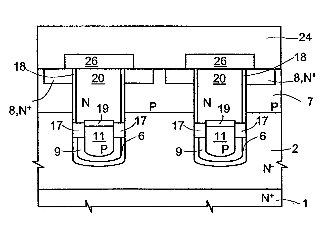
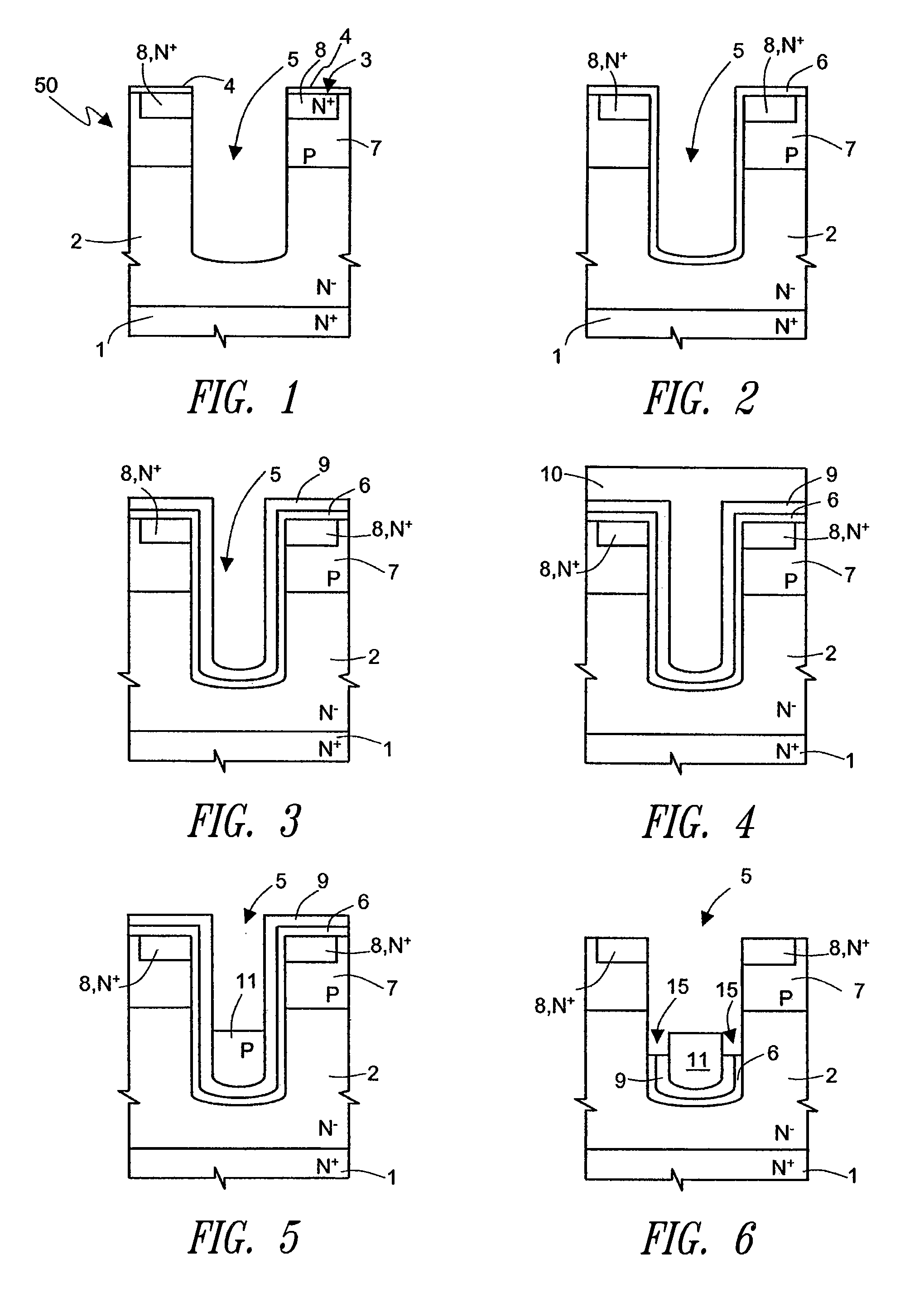
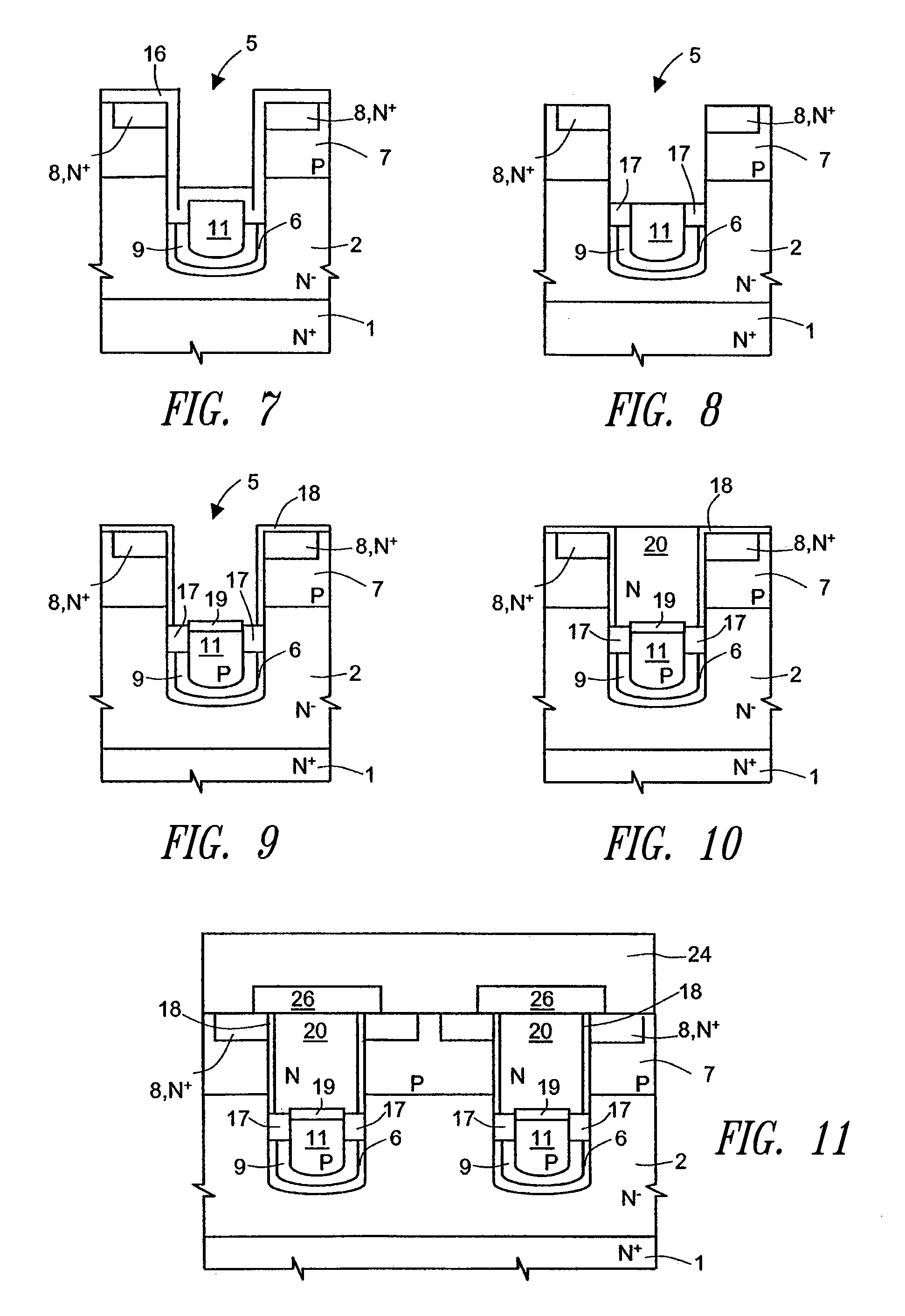
[0025]FIG. 1 shows a wafer 50 of semiconductor material that comprises a substrate 1, which is heavily doped (for example, of an N+ type for forming a power MOS or P+ type for forming an IGBT), and a semiconductor layer, which is less doped (in the example, of an N-type) and is, for example, grown epitaxially on top of the substrate 1 (epitaxial layer 2 forming a drift region). The epitaxial layer has a top surface 3, and a buffer layer, for example of an N+ type, can extend between the substrate 1 and the epitaxial layer 2.

[0026] After manufacturing edge structures and opening the active area, body regions 7 of P-type are blanket-implanted, for example, by doping the silicon with B, BF2, Al, or In. In a way not shown, a deep enrichment of the body regions (deep body) is possibly effected in accordance with the prior art, by implanting dopants of P+ type using a resist mask; then, using another resist mask, source regions 8 of N+ type are implanted, for example, by doping silicon w...


PUM


Abstract

A semiconductor power device has a semiconductor body with a first conductivity type. A trench extends in the semiconductor body and accommodates an insulating structure, which extends along the side walls and bottom of the trench. The insulating structure surrounds a conductive region, arranged on the bottom of the trench, and a gate region, arranged on top of the conductive region, the conductive region and the gate region being electrically insulated by an insulating layer. A body region, with a second conductivity type, extends within the semiconductor body, at the sides of the trench, and a source region, with the first conductivity type, extends within the semiconductor body, at the sides of the trench and within the body region. The conductive region and the gate region are both of polycrystalline silicon but have different conductivities and doping levels so as to have different electrical characteristics such as to improve the static and dynamic behaviour of the device.

Description

BACKGROUND OF THE INVENTION [0001] 1. Field of the Invention [0002] The present invention relates to an insulated-gate semiconductor power device and to the manufacturing process thereof. More specifically, the invention relates to a power MOS device of the type comprising a trench used for insulating the gate region of the device (hereinafter indicated as power MOS device of the trench-gate type). [0003] The invention relates, in particular, but not exclusively, to a power MOS device or a device of the IGBT (Insulated-Gate Bipolar Transistor) type, and the following description is made with reference to this application field, with the only purpose of simplifying its exposition. [0004] 2. Description of the Related Art [0005] As is known, power MOS devices comprise a plurality of cells, each having a gate region adjacent to body and source regions. In the manufacturing process of trench-gate power MOS devices, the gate of the MOS structure is formed in each elementary cell of the d...

Claims


Application Information

Patent Timeline
IPC IPC(8): H01L29/94
CPCH01L29/0623H01L29/0878H01L29/407H01L29/42368H01L29/7813H01L29/512H01L29/513H01L29/66727H01L29/66734H01L29/4933
Inventor ARENA, GIUSEPPECAMALLERI, CATENO MARCOFORTUNA, STEFANIAMAGRI, ANGELO
Owner STMICROELECTRONICS SRL
Why Eureka
Try Eureka