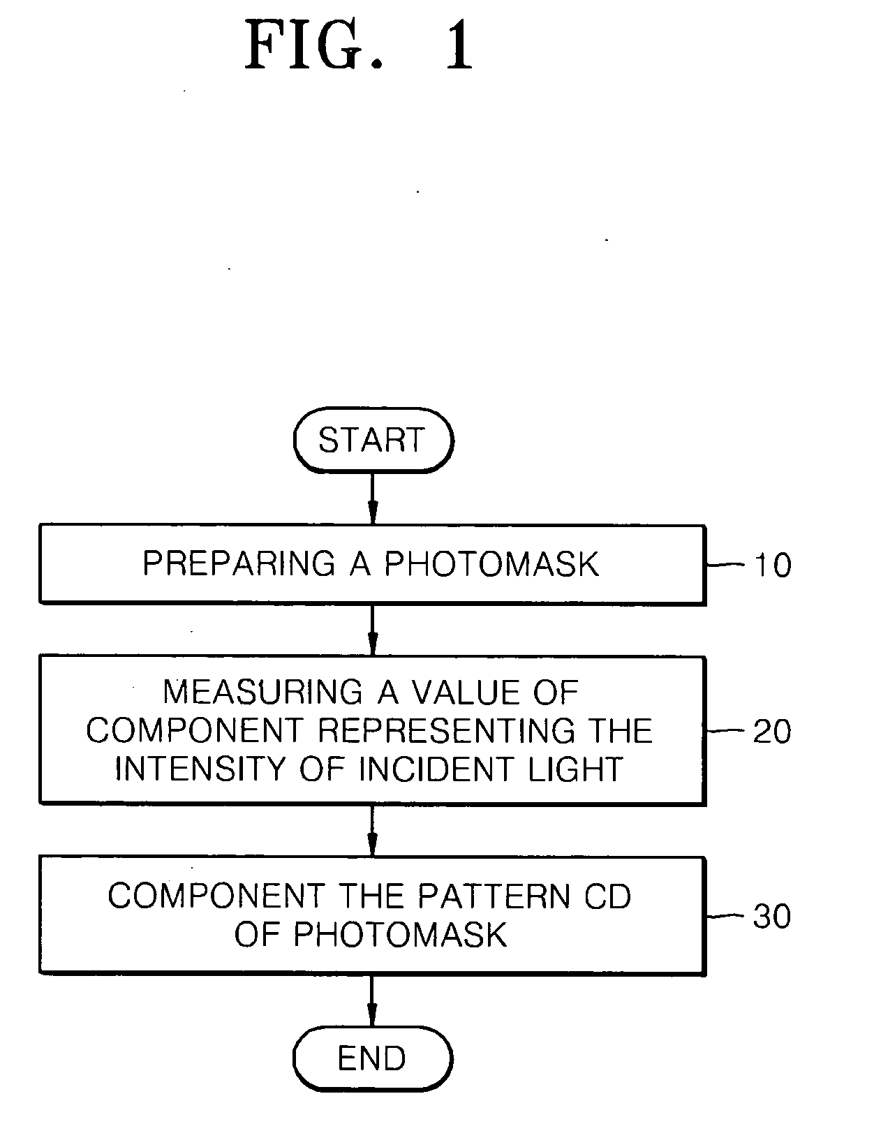
Photomask providing uniform critical dimension on semiconductor device and method of manufacturing the same
a technology of critical dimension and photomask, which is applied in the field of photomasks, can solve the problems of multi-circuit die formation and the rise of intra-die cd non-uniformity as a more dominant source of error
- Summary
- Abstract
- Description
- Claims
- Application Information
AI Technical Summary
Benefits of technology
Problems solved by technology
Method used
Image

Examples
Embodiment Construction
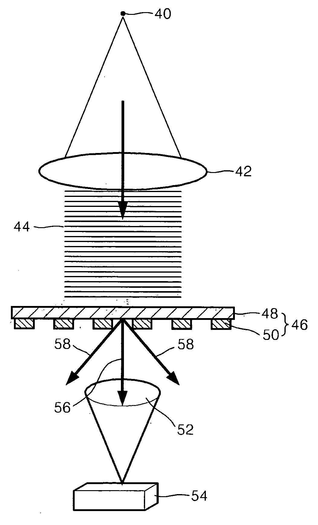
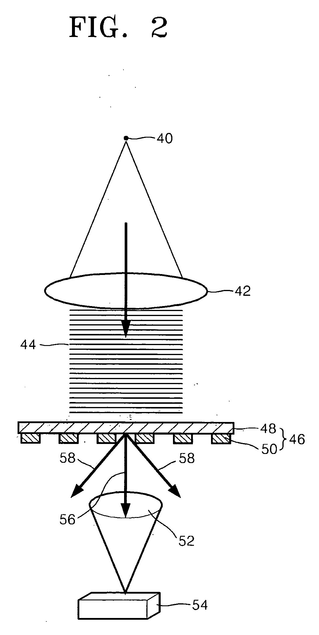
[0047] In the following description, when a layer is described as being formed on another layer or on a substrate, the layer may be formed on the other layer or on the substrate, or a third layer may be interposed between the layer and the other layer or the substrate.
[0048] Typically, CD non-uniformity in a wafer can be caused by various sources of error. These include the exposure tool, the wafer substrate, the wafer production process, the mask or reticle and other sources of error. These sources of error have an effect on the CD uniformity budget run-to-run (R2R), that is, over multiple groups of wafers processed in multiple respective production runs; wafer-to-wafer, that is, over multiple wafers within a single run; intra-wafer, that is, within a single wafer; and intra-die, that is, within a single die on a wafer. The present invention mitigates intra-die CD non-uniformity by correcting sources of error in the mask or reticle.
[0049] Typically, spatial distribution error in ...
PUM
| Property | Measurement | Unit |
|---|---|---|
| angle of incidence | aaaaa | aaaaa |
| angle of incidence | aaaaa | aaaaa |
| incidence angle | aaaaa | aaaaa |
Abstract
Description
Claims
Application Information
 - Generate Ideas
- Intellectual Property
- Life Sciences
- Materials
- Tech Scout
- Unparalleled Data Quality
- Higher Quality Content
- 60% Fewer Hallucinations
Browse by: Latest US Patents, China's latest patents, Technical Efficacy Thesaurus, Application Domain, Technology Topic, Popular Technical Reports.
© 2025 PatSnap. All rights reserved.Legal|Privacy policy|Modern Slavery Act Transparency Statement|Sitemap|About US| Contact US: help@patsnap.com