

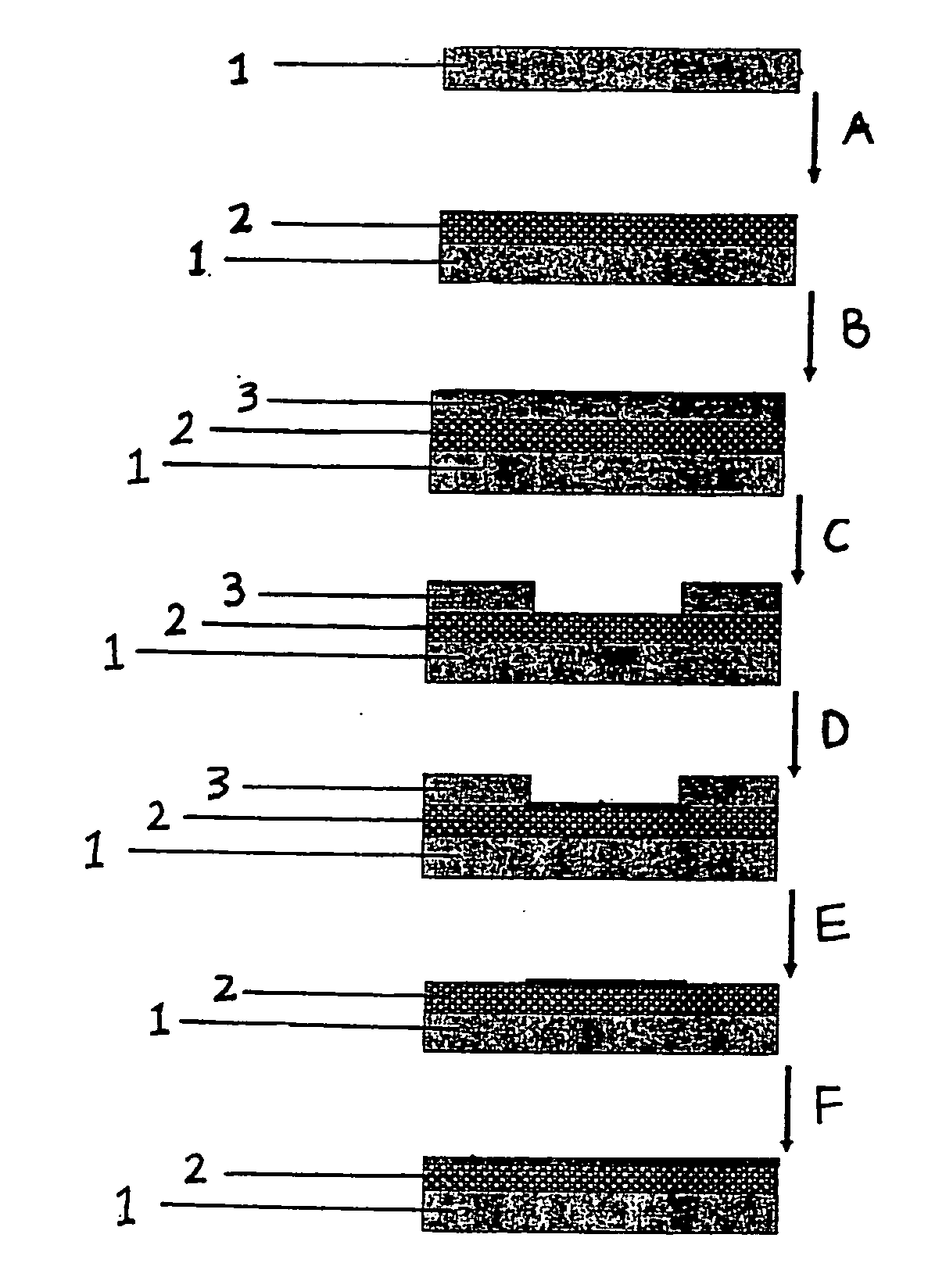
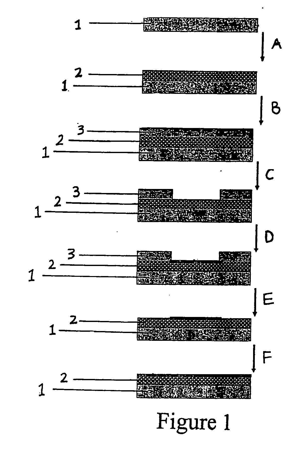
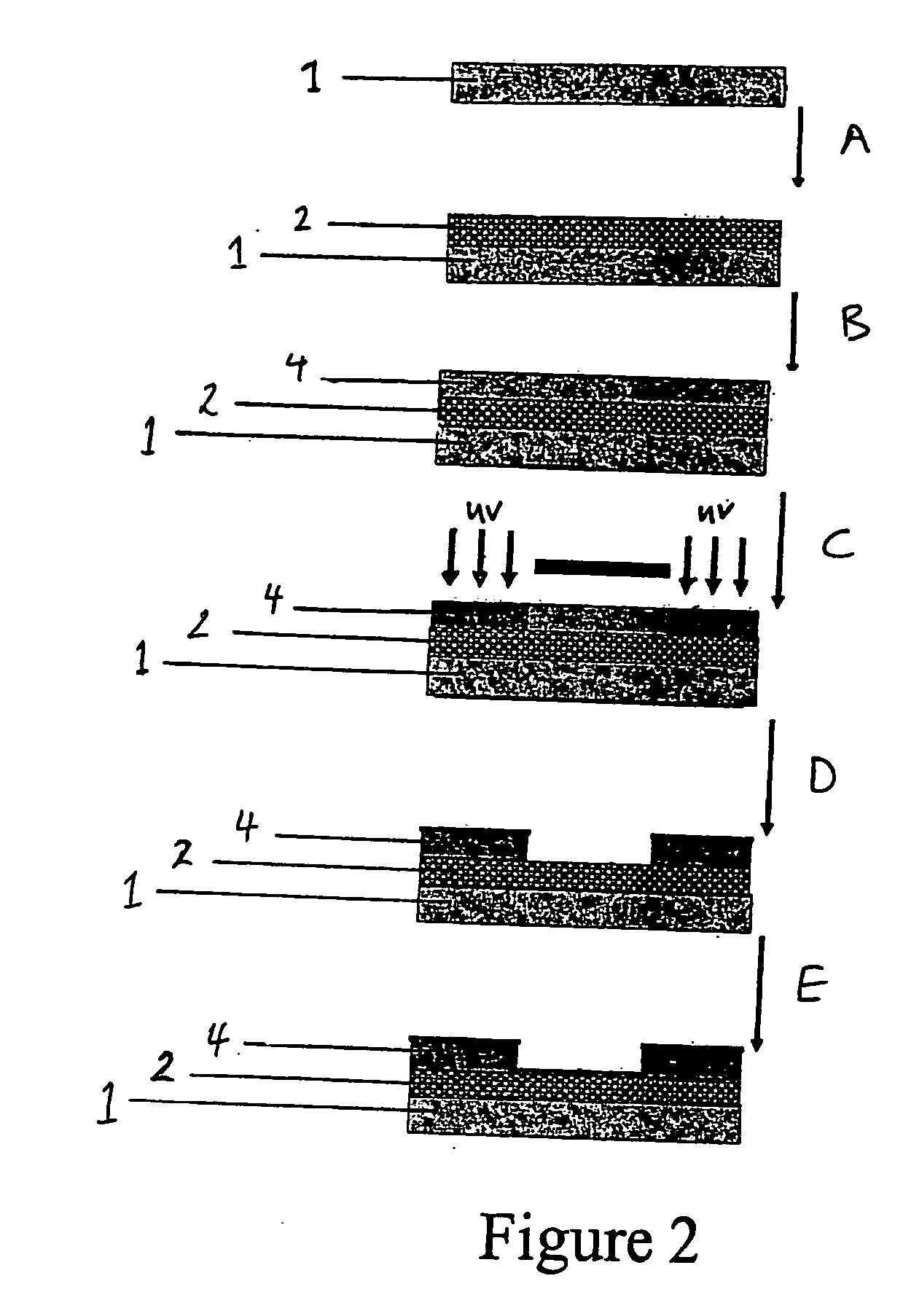
Method of producing a substrate having areas of different hydrophilicity and/or oleophilicity on the same surface
a technology of hydrophilicity and oleophilicity on the same surface, applied in the direction of conductive pattern formation, sustainable manufacturing/processing, final product manufacturing, etc., can solve the problems of insufficient resolution of ink-jet printing, inability to carry out this in practice, and high cos
- Summary
- Abstract
- Description
- Claims
- Application Information
AI Technical Summary
Benefits of technology
Problems solved by technology
Method used
Image

Examples
example 1
Modification of Surface Properties by Plasma Treatment
[0108] Preparation of substrates
[0109] Reference substrate
[0110] A 3% polymethylmethacrylate (PMMA) solution in butylacetate was prepared by dissolving 0.93 g of PMMA (from Sigma Aldrich) in 30 ml butylacetate. 0.5 ml of the solution was spin coated onto a glass substrate (12×12mm) precursor (7059 from Corning) for 30 seconds at 1500 rpm in air. The coated precursor was then annealed for 10 minutes at 100° C. in air to form a Reference Substrate.
[0111] Substrate 1
[0112] 0.028g of nanoparticulate SiO2 (hexamethyldisilazane treated silica particles, 10-20nm, from ABCR) was dispersed in 1 ml 6% PMMA in butylacetate (Aldrich) and 1 ml butylacetate (Aldrich). The mixture was mixed thoroughly by stirring on a magnetic stirrer and by a final ultrasonic mixing step in an ultrasonic bath for 5 minutes to yield a solution comprising 17.3 vol. % SiO2. 0.5 ml of the solution was spin coated onto a glass substrate precursor (12×12 mm pla...
example 2
Modification of Surface Properties by Silanisation with a Fluoroalkylsilane
[0127] Preparation of substrates
A Reference Substrate and Substrates 1-5 were Prepared as in Example 1 above.
[0128] Plasma treatment and measurements
[0129] Substrates 1-5 and the Reference Substrate were rinsed with water. Then the contact angles with water were measured for each of these six substrates using a goniometer (contact angle measuring device) with droplet size 1-5 μl.
[0130] Subsequently, each of the six substrates was exposed to a CF4 plasma treatment in a Branson / IPC Series S2100 Plasma Stripper system for 7 seconds at a flow rate of 200 ml / min and at a power of 200W. Contact angles of the treated substrates were measured using the same apparatus and methods as above. In the substrates with high oxide content (B4 and B5), the inventors observed a fast initial decrease of the contact angles, with the values slowly stabilising after prolonged measurement times. Thus, the contact angle ranges ...
PUM
| Property | Measurement | Unit |
|---|---|---|
| particle size | aaaaa | aaaaa |
| contact angles | aaaaa | aaaaa |
| contact angles | aaaaa | aaaaa |
Abstract
Description
Claims
Application Information