Flat panel display and method for manufacturing the same

a technology of flat panel display and manufacturing method, which is applied in the field of flat panel display, can solve the problems of difficult control of the arrangement of nano-particles in the channel region, insufficient performance of organic thin film transistor, etc., and achieves the effects of high picture quality, high electrical mobility, and high flexibility

Inactive Publication Date: 2007-03-29
PANASONIC CORP
View PDF9 Cites 58 Cited by
  • Summary
  • Abstract
  • Description
  • Claims
  • Application Information

AI Technical Summary

Benefits of technology

[0011] It is therefore an object of the present invention to provide a flat panel display having high picture quality, high flexibility, and high flex-resistance.
[0012] The present inventors have discovered that a thin film transistor having a channel region containing nanowire where the axial direction of the nanowire is arranged in the same direction as the source-drain direction is difficult to be damaged even if the transistor is bent so as to intersect with the axial direction of the nanowire (i.e. source-drain direction). Then, the inventors have arrived at the present invention by applying this knowledge to a flexible flat panel display.
[0031] applying a potential difference between the region to be the channel and the paste that are in close proximity to each other, increasing wettability of the paste and transferring the paste from the printing plate to the region to be the channel, wherein the axial direction of the nanowire, nanorod, nanoribbon or nanotube is arranged in the same direction as the source-drain direction of the channel region.
[0044] applying a potential difference between the region to be the channel and the paste that are in close proximity to each other, increasing wettability of the paste and transferring the paste from the printing plate to the region to be the channel, wherein the axial direction of the nanowire, nanorod, nanoribbon or nanotube is arranged in the same direction as the source-drain direction of the channel region.
[0045] The flat panel display of the present invention is provided with thin film transistor having a channel region containing nanowire of high electrical mobility so that high picture quality can be achieved. Further, the flat panel display of the present invention is bendable so as to intersect with the axial direction of nanowire etc. contained in the channel region of thin film transistor (i.e. is bendable so as to intersect with the source-drain direction of the channel region), so that the panel has a higher flexibility, and is more difficult to be damaged due to bending. The flat panel display of the present invention can be applied to, for example, roll screen.

Problems solved by technology

Therefore, there is a case where the performance of organic thin film transistor is not sufficient.
However, in general, it has been difficult to control the arrangement of nano-particle in channel region.

Method used


Image

  • Flat panel display and method for manufacturing the same
  • Flat panel display and method for manufacturing the same
  • Flat panel display and method for manufacturing the same

Examples


Embodiment Construction

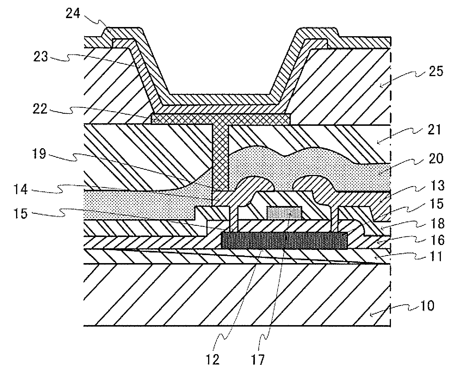
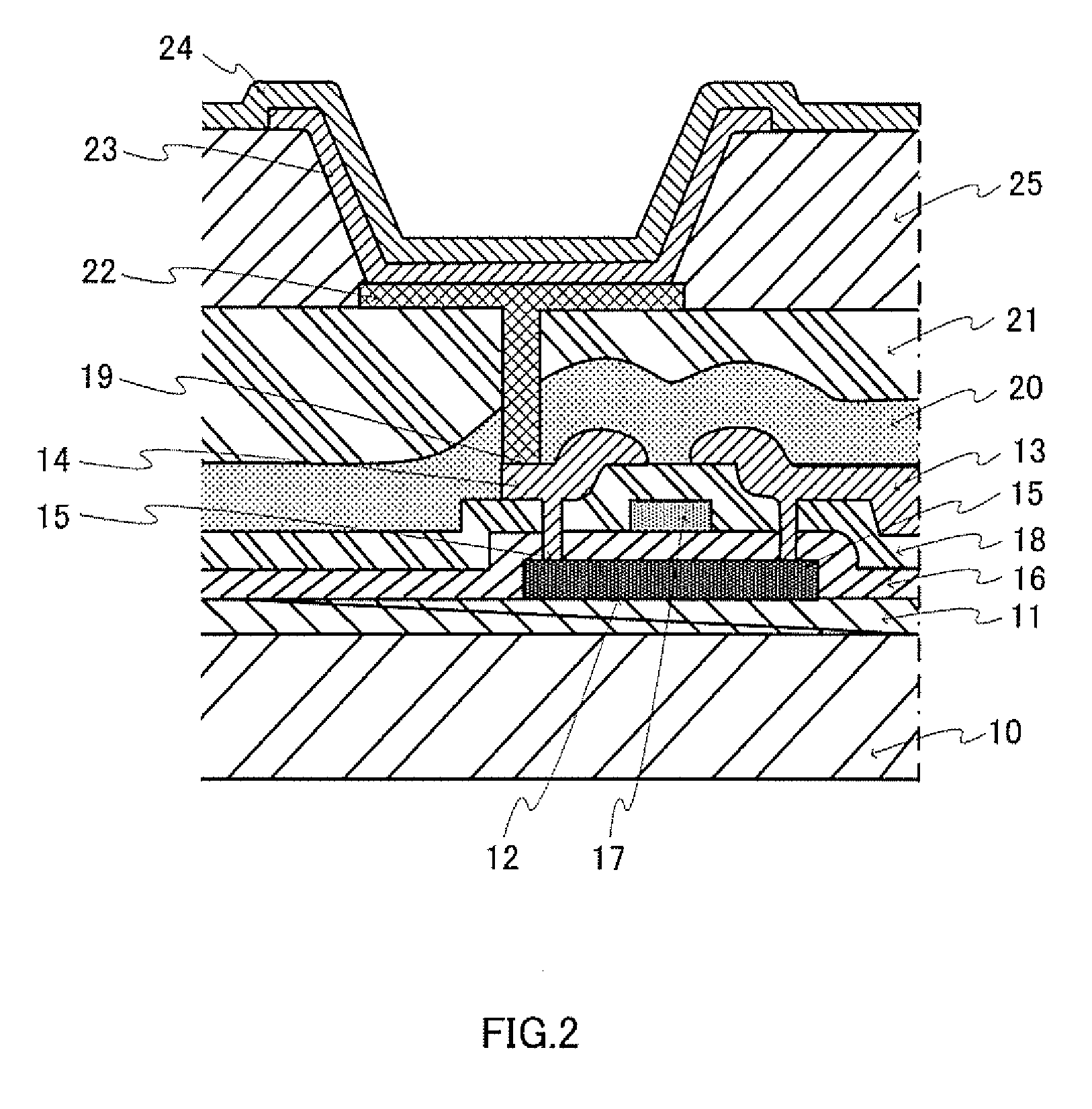
1. Flat Panel Display of the Present Invention.

[0052] The flat panel display of the present invention is provided with a plurality of pixels arranged in a matrix shape on a substrate, and is a display panel referred to as an active type, where a thin film transistor for driving is incorporated at each pixel. The number of pixels arranged on the substrate is not particularly limited, and may be decided appropriately according to the desired performance of the display apparatus. An example of a flat panel display includes organic EL display and liquid crystal display.

[0053] The flat panel display of the present invention has flexibility and is bendable so that it is preferable that the material of the substrate the pixels are arranged on is a material with flexibility. An example of a material with flexibility may include a plastic material, and an example of a plastic material may include acrylic-resin, polyimide, polycarbonate, polyester, poly(ethylene terephthalate), or poly(eth...


PUM


Abstract

The present invention relates to a flat panel display having high picture quality, high flexibility and high flex-resistance. Specifically, the present invention provides a flat panel display having a plurality of pixels arranged in a matrix shape on a substrate, each of the plurality of pixels comprising a thin film transistor having a channel region containing nanowire, nanorod, nanoribbon, or nanotube, and a display element driven by the thin film transistor. Here, an axial direction of the nanowire, nanorod, nanoribbon, or nanotube is in the same direction as the source-drain direction of a channel region and the flat panel display can be bent so as to intersect with the source-drain direction.

Description

CROSS REFERENCE TO RELATED APPLICATION [0001] This application claims priority based on Japanese Patent Application No. 2005-284325 filed on Sep. 29, 2005. The entire content disclosed in the specification of the aforementioned application is incorporated in the specification of this application. BACKGROUND OF THE INVENTION [0002] 1. Field of the Invention [0003] The present invention relates to a flat panel display, and more particularly to a flexible flat panel display. [0004] 2. Description of the Related Art [0005] In recent years, flat panel display such as organic EL display and liquid crystal display etc. is required for not only thin-model and miniaturization, but also properties (flexibility) capable of being folded or rolled up for easier portability. [0006] On the other hand, high picture quality is also required for flat panel display. In order to attain high picture quality, an active drive scheme incorporating transistor for driving to each pixel is adopted. It is pref...

Claims


Application Information

Patent Timeline
Patent Type & Authority Applications(United States)
IPC IPC(8): H01L29/04
CPCB82Y10/00H01L27/1214H01L27/3262H01L2251/5338H01L29/78681H01L29/78696H01L51/0048H01L29/0673H01L27/127H01L27/1225H01L27/1222H10K59/1213H10K85/221H10K2102/311
Inventor SAITOH, MITSUOYOSHIDA, HIDEHIRO
Owner PANASONIC CORP
Why Eureka
Try Eureka