Test mode controller

a controller and test mode technology, applied in the field of test mode controllers, can solve the problems of unnecessari consumption of burn-in test time, inability to repair the wafer chip, and inability to use the chip, so as to reduce the area of the chip and unnecessary current consumption, and achieve the effect of simple structur

Inactive Publication Date: 2007-03-29
SK HYNIX INC
View PDF7 Cites 2 Cited by
  • Summary
  • Abstract
  • Description
  • Claims
  • Application Information

AI Technical Summary

Benefits of technology

[0024] It is, therefore, an object of the present invention to provide a test mode controller in which output signals of wafer burn-in test and programmable stress test circuits are output as one output signal through a circuit having a relatively simple structure, capable of reducing a chip area and unnecessary current consumption by integrally constructing latch units of the two test circuits.

Problems solved by technology

However, if there is a significant number of detects corresponding to several bits or higher, it is impossible to repair the wafer chip.
Thus, this chip cannot be used.
As a result, the package cost of the chip and the time for the burn-in test after packaging have been unnecessarily consumed.
In addition, this problem may becomes more serious in a highly integrated device so that the burn-in test becomes more and more important in order to accurately detect the defective cells vulnerable to the wafer burn-in test before the package process.
Therefore, an unnecessary circuit is used in the conventional test mode controller.
The conventional test mode controller requires a large chip area, high current consumption, and limited operational speed.

Method used


Image

  • Test mode controller
  • Test mode controller
  • Test mode controller

Examples


Embodiment Construction

[0034] A test mode controller in accordance with exemplary embodiments of the present invention will be described in detail with reference to the accompanying drawings.

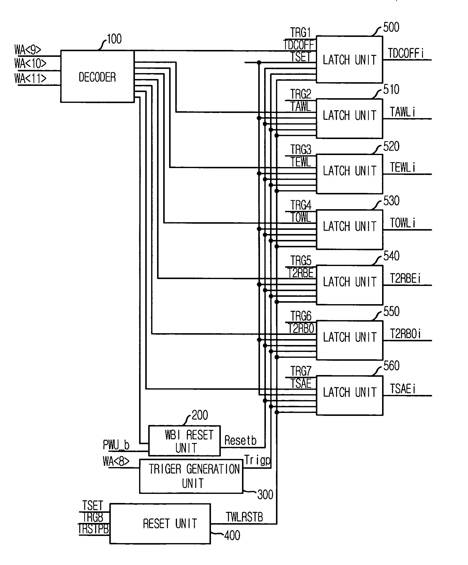
[0035]FIG. 5 is a block diagram of a test mode controller in accordance with the present invention.

[0036] Referring to FIG. 5, the test mode controller of the present invention includes a decoder 100, a wafer burn-in (WBI) reset unit 200, a trigger generation unit 300, a reset unit 400 and a plurality of latch units 500 to 560.

[0037] The decoder 100 decodes input signals WA9>, WA10> and WA activated in a wafer burn-in test so as to output test mode setting signals TDCOFF, TAWL, TEWL, TOWL, T2RBE, T2RBO and TSAE.

[0038] Herein, the test mode setting signal TAWL is a signal for testing all the word lines. The test mode setting signal TEWL is a signal for testing even-number of word lines (0, 2, 4, 6, . . . ), whereas the test mode setting signal TOWL is a signal for testing odd-number of word lines (0, 1, 3, 5, . . ....


PUM


Abstract

A test mode controller is capable of reducing a chip area and unnecessary current consumption by integrally constructing latch units of the two test circuits. The test mode controller includes a test control block for determining a test mode between a programmable test and a wafer burn-in test to generate a reset signal and a control signal generating block for receiving a plurality of input signals activated in a wafer burn-in test to generate a plurality of test control signals in response to the reset signal and a programmable test signal activated in a programmable stress test.

Description

FIELD OF THE INVENTION [0001] The present invention relates to a test mode controller; and, more particularly, to a test mode controller capable of reducing a chip area and current consumption by integrally constructing circuitry for performing a wafer burn-in test and a programmable stress test for testing the reliability. BACKGROUND [0002] In general, tests are mainly classified into two types, i.e., product tests and prove (or function) tests. The product test screens for product failures and sorts out articles of good quality from defects that can occur during wafer-processing, an assembly process, etc. [0003] The prove test confirms whether or not the function or performance of a manufactured DRAM meets design specification. The product test is frequently performed during a shipping process, and thus there is required high throughput in the product test. The purpose of the prove test is to shorten a development period and raise the completion degree of the product by thoroughly...

Claims


Application Information

Patent Timeline
Patent Type & Authority Applications(United States)
IPC IPC(8): G11C29/00
CPCG11C29/006G11C29/46G11C29/14
Inventor OH, SEUNG-MIN
Owner SK HYNIX INC
Why Eureka
Try Eureka