ADC architecture for wireless applications

a wireless application and adc architecture technology, applied in the field of wireless communication, can solve the problems of high-performance adc circuits, high-power consumption adc circuits, and the pair of adc circuits, and achieve the effects of reducing circuit size and power, reducing circuit area and power consumption, and reducing the number

Active Publication Date: 2008-06-17
MARVELL ASIA PTE LTD
View PDF22 Cites 21 Cited by
  • Summary
  • Abstract
  • Description
  • Claims
  • Application Information

AI Technical Summary

Benefits of technology

[0011]One aspect of the present invention is an improved baseband circuit for use in connection with an RF receiver for wireless communication of data. The new baseband circuit provides a substantial reduction in circuit area and power consumption by reducing the number of ADC circuits necessary for conversion of analog data streams. According to one embodiment, the receiver provides “i” and “q” orthogonal analog signals from corresponding demodulators. These two signals are converted to digital data in a single, shared ADC circuit, thereby substantially reducing circuit size and power.

Problems solved by technology

One significant drawback of the receiver architecture summarized above is related to the pair of ADC circuits.
Especially in pipelined converter designs, offset, gain errors and other imperfections in the ADC circuits add to their complexity.
Consequently, high performance ADC circuits are expensive both in terms of chip area and power consumption.

Method used


Image

  • ADC architecture for wireless applications
  • ADC architecture for wireless applications
  • ADC architecture for wireless applications

Examples


Embodiment Construction

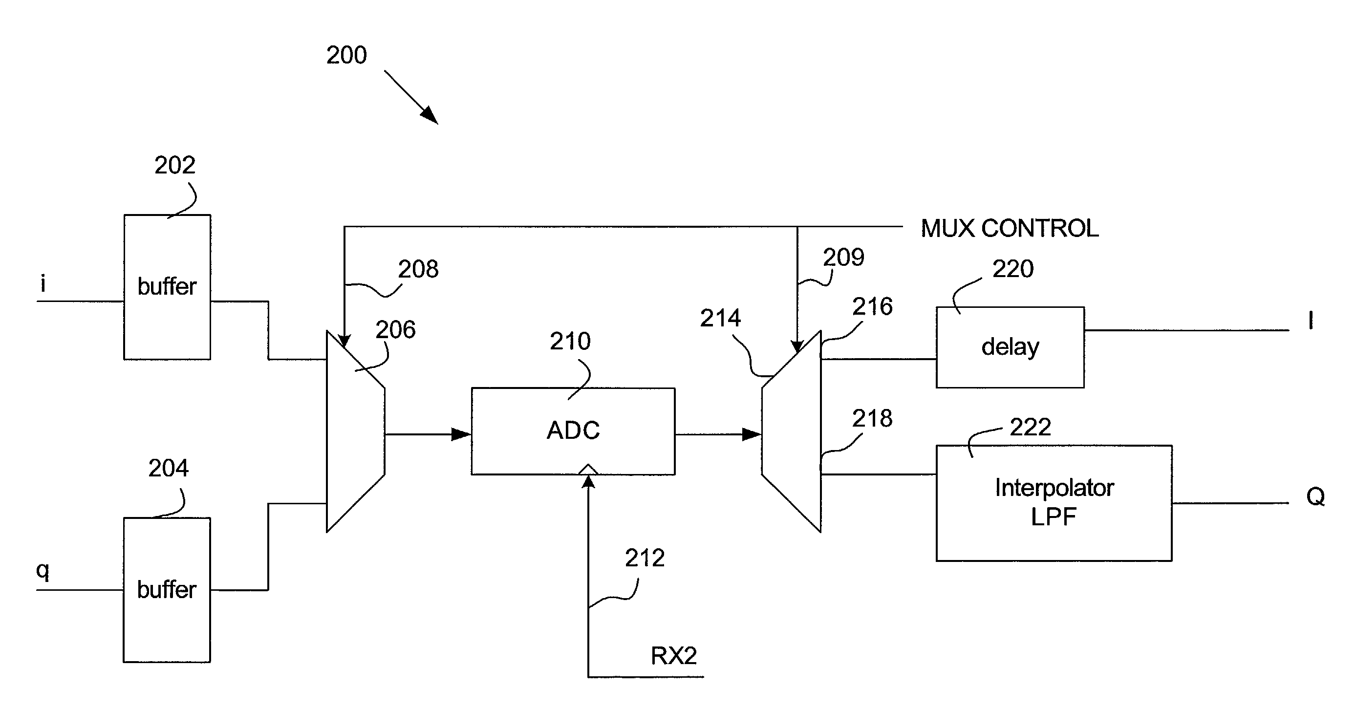
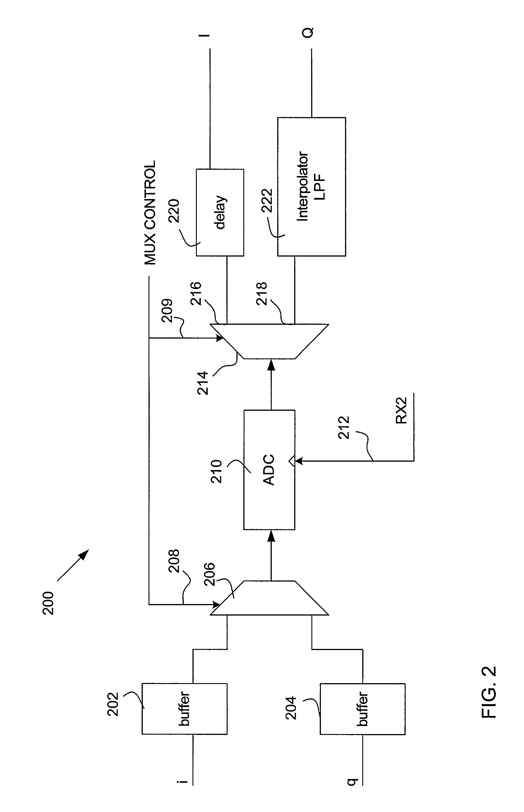
[0023]The present invention is directed to improvements in receiver circuits generally of the type illustrated in FIG. 1. It is not limited to 2-D modulation, however, but could be used in any multi-dimensional modulation RF communications application. For simplicity, we describe below particular embodiments of the invention, directed to a 2-D (I,Q) modulation application.

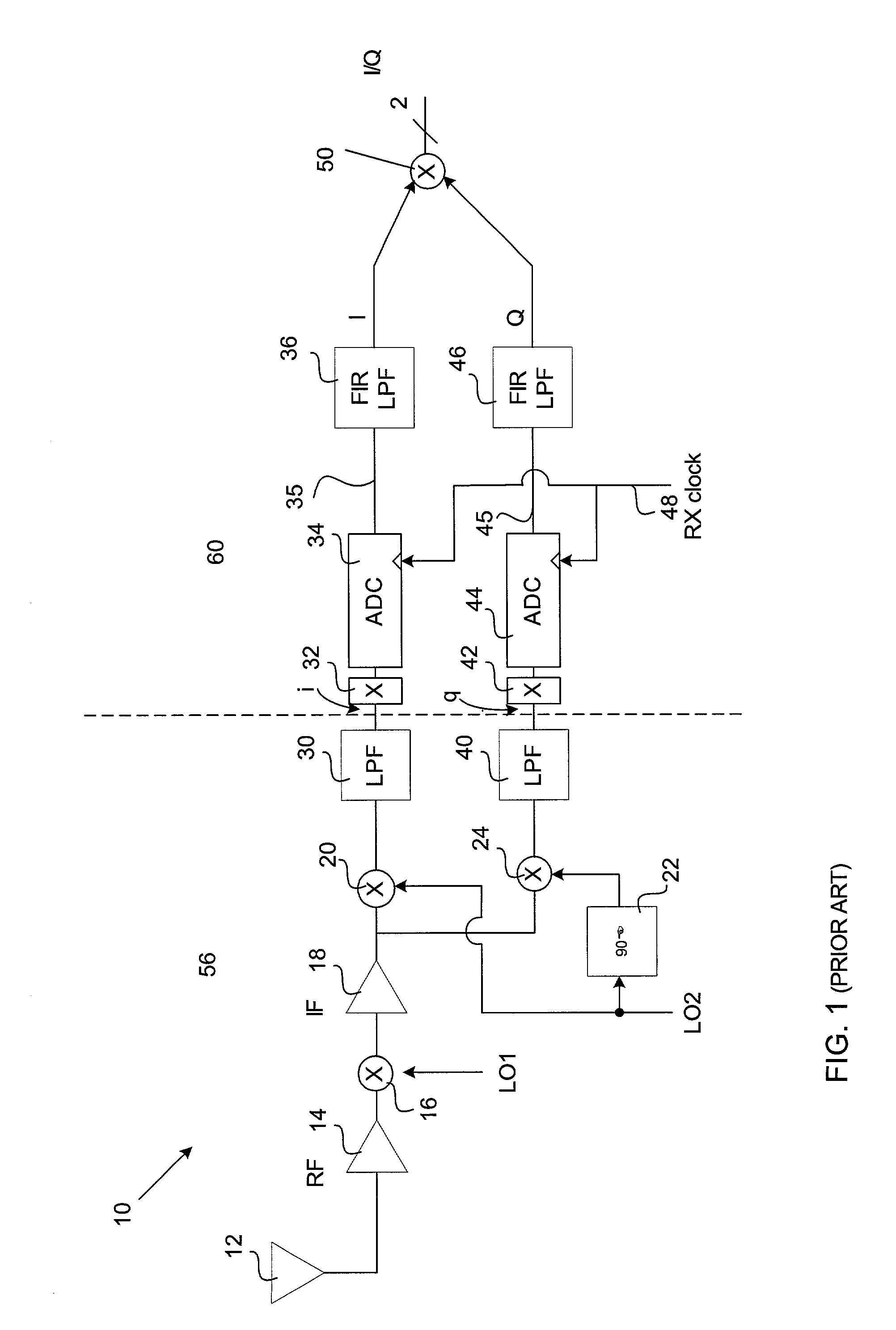
[0024]As described above with reference to FIG. 1, a typical RF or wireless communications receiver includes RF input, filtering, down-mixing etc. all generally designed to recover the I and Q analog signals. We will refer to such circuitry as the RF portion of the receiver, although it includes IF operations as well. Using this working definition, the RF portion provides the baseband analog signals i, q at its output. The RF portion 56 of the receiver of FIG. 1 is the circuitry generally to the left of the dashed line.

[0025]The circuitry60 on the right side of FIG. 1, including in particular the pair of ADCs, proc...


PUM


Abstract

A simplified architecture is disclosed for ADC conversion of received in-phase I and quadrature Q signals. Circuit area is substantially reduced by sharing a single ADC to convert both signals, switching the ADC input alternately between the i and q signals. In an embodiment, the ADC is clocked at an increased sample rate, and the digital output signals are aligned to compensate for the phase difference resulting from the implementation of a single ADC. Aligning includes delaying one of the digital signals, and interpolating the other one of the digital signals in a low pass filter so as to compensate for the phase difference introduced by the sampling during the first and second time intervals. The first and second time intervals are equal to a predetermined ADC sample period corresponding to a sample clock cycle. Delaying the first digital signal includes a delay of 1/2 clock cycle.

Description

TECHNICAL FIELD[0001]This invention pertains to wireless communications and, more specifically, to improved methods and apparatus for analog to digital conversion in a voice and / or data communication receiver.BACKGROUND OF THE INVENTION[0002]Most wireless receiver circuits employ similar architectures. On the transmitter side (not shown), digital user data (which may be encoded or sampled voice data) is input to a bit-symbol encoder, which may be implemented as a dedicated circuit or a combination of hardware and software (such as a DSP). In any event, the bit-symbol encoder typically splits the data into two half-rate streams. These streams are modulated onto a pair of orthogonal carriers, called I and Q for in-phase and quadrature-phase carriers respectively, although other modulation schemes are known. This is a 2-D (or two-dimensional) transmission scheme. The I and Q signals are combined for transmission over an RF channel as is well known in the art.[0003]Referring now to FIG....

Claims


Application Information

Patent Timeline
Patent Type & Authority Patents(United States)
IPC IPC(8): H04L27/00H04B7/12H04L27/06H04L7/00
CPCH03M1/1225H04L27/38
Inventor HSU, YUNGPINGYU, MAO
Owner MARVELL ASIA PTE LTD
Why Eureka
Try Eureka