Arrayed waveguide grating device

Inactive Publication Date: 2007-03-29
NAT CENT UNIV
View PDF5 Cites 20 Cited by
  • Summary
  • Abstract
  • Description
  • Claims
  • Application Information

AI Technical Summary

Benefits of technology

[0008] In addition, the taper optical attenuator comprises a taper waveguide where a third input waveguide is connected to a front-end of the taper waveguide and a third output waveguide is connected to a back-end of the taper waveguide. Because the taper waveguide enlarges the optical field inputted, an optical loss occurs when coupling to the third output waveguide to obtain a

Problems solved by technology

Because the taper waveguide enlarges the optical field inputted, an optical loss

Method used


Image

  • Arrayed waveguide grating device
  • Arrayed waveguide grating device
  • Arrayed waveguide grating device

Examples


Embodiment Construction

[0031] The following descriptions of the preferred embodiments are provided to understand the features and the structures of the present invention.

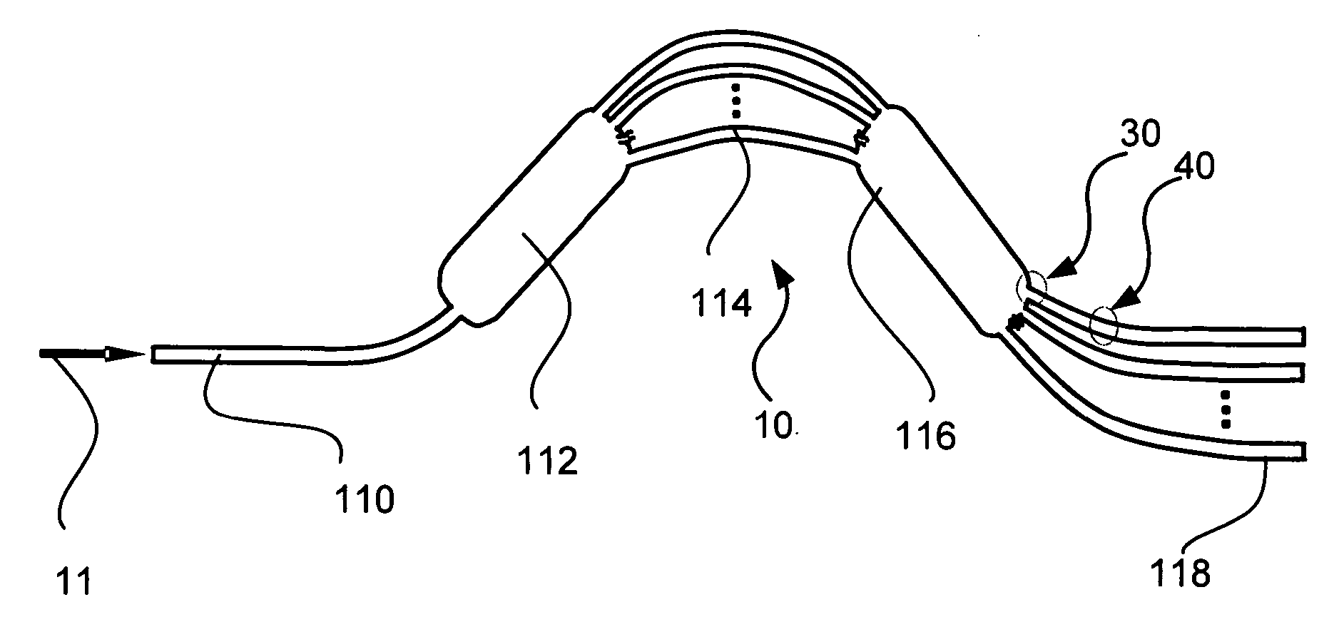
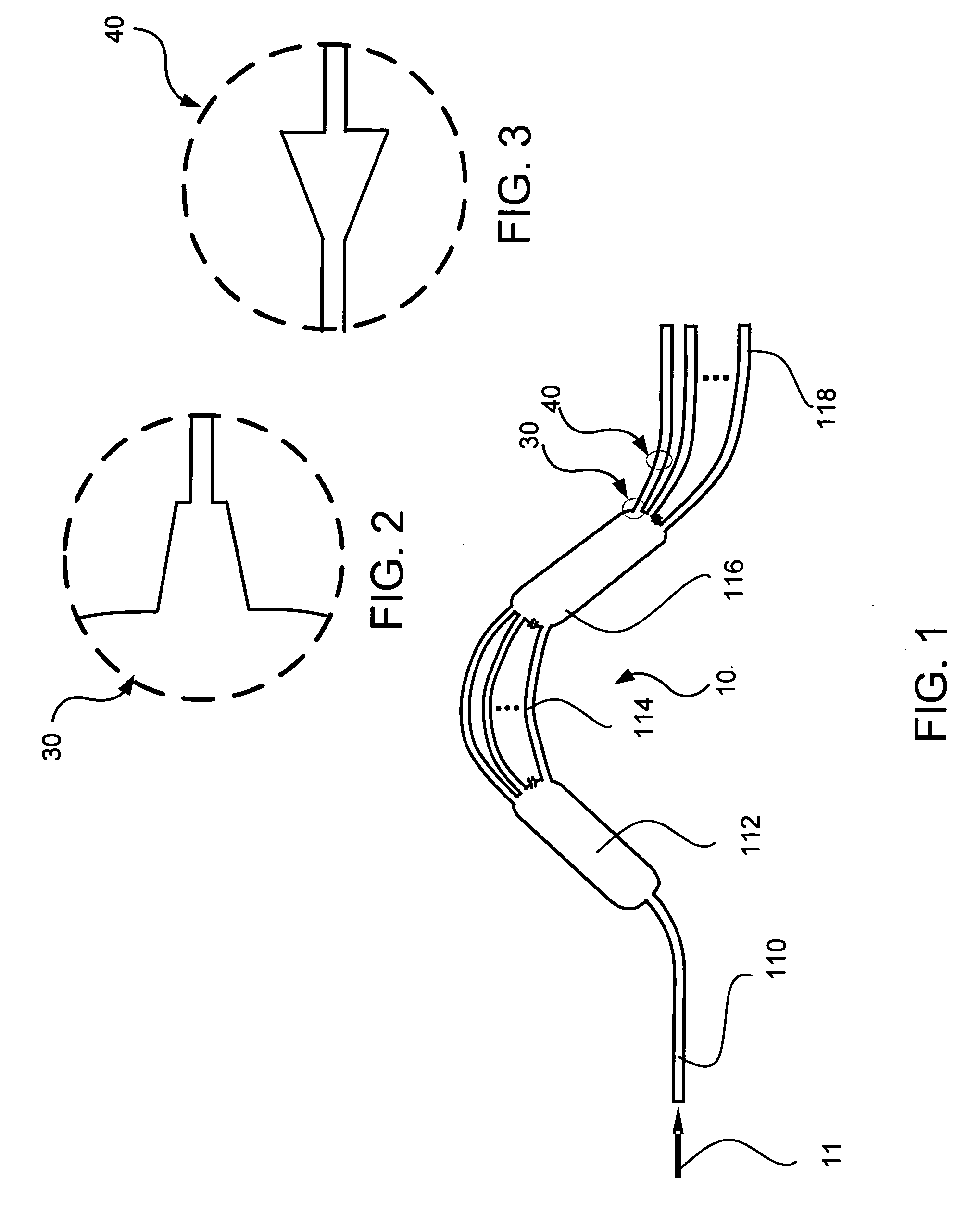
[0032] Please refer to FIG. 1, through FIG. 4, which are a structural view showing an AWG device, a taper MMI coupler of the AWG device, a taper optical attenuator of the AWG device and an enlarged top view showing an OIC of an AWG device, according to the present invention. As shown in FIG. 1, the present invention is an AWG device, comprising an AWG member 10, a taper MMI coupler 30 (as shown in FIG. 2) and a taper optical attenuator 40 (as shown in FIG. 3). The AWG device can be an optical router (i.e. a wave length router) or an WDM. An optical wavelength appears periodically with intervals of a free spectral range (FSR) according to the passband. Yet, such a phenomenon does not happen to an WDM. Hence, an optical wavelength is expressed as λaN+1, λaN+2, . . . , where, for an WDM, a is 0; and, for an optical router, a is an integer a...


PUM


Abstract

The present invention comprises an arrayed waveguide grating member, a taper multimode interference coupler and a taper optical attenuator to uniform and flatten a passband in an optical device.

Description

FIELD OF THE INVENTION [0001] The present invention relates to an arrayed waveguide grating (AWG); more particularly, relates to utilizing an AWG member, a taper MMI coupler and a taper optical attenuator to obtain a uniformed and flattened passband in an optical device. DESCRIPTION OF THE RELATED ARTS [0002] In a traditional system of an AWG device, no matter a wavelength division multiplexer / demultiplexer (WDM) or an optical router, the passband comprises a distribution like a Gaussian function. Hence, an accuracy on wavelength of a laser source for the system is quite demanding so that a laser source with high wavelength accuracy is used and so the cost of the system is greatly increased. In addition, the passbands are not flat and the uniformities between the passbands are not good in an optical router. For an optical communication system, a cheaper laser diode is used as a laser source under a consideration of cost. Yet, after optical signals of laser have passed the AWG, the o...

Claims


Application Information

Patent Timeline
IPC IPC(8): G02B6/34G02B6/10G02B6/42G02B6/26
CPCG02B6/12016G02B6/12019G02B6/266
Inventor LU, HUNG-CHIH
Owner NAT CENT UNIV
Why Eureka
Try Eureka