Method for reducing positive charges accumulated on chips during ion implantation

a technology of ion implantation and positive charges, which is applied in the direction of semiconductor devices, electrical equipment, basic electric elements, etc., can solve the problem that the production of electrons is not sufficient to completely neutralize the accumulated positive charges, and achieve the effect of alleviating the volcano effects of accumulated charges

Inactive Publication Date: 2007-03-29
UNITED MICROELECTRONICS CORP
View PDF2 Cites 3 Cited by
  • Summary
  • Abstract
  • Description
  • Claims
  • Application Information

AI Technical Summary

Benefits of technology

[0015] By using the conductive photoresist pattern as a mask for one or more ion implantation processes, the positive charges accumulated during the i...

Problems solved by technology

However, if the current of the ion beam is not large enough, the produced ele...

Method used


Image

  • Method for reducing positive charges accumulated on chips during ion implantation
  • Method for reducing positive charges accumulated on chips during ion implantation
  • Method for reducing positive charges accumulated on chips during ion implantation

Examples


Embodiment Construction

[0022] Reference will now be made in detail to the present preferred embodiments of the invention, examples of which are illustrated in the accompanying drawings. Wherever possible, the same reference numbers are used in the drawings and the description to refer to the same or like parts.

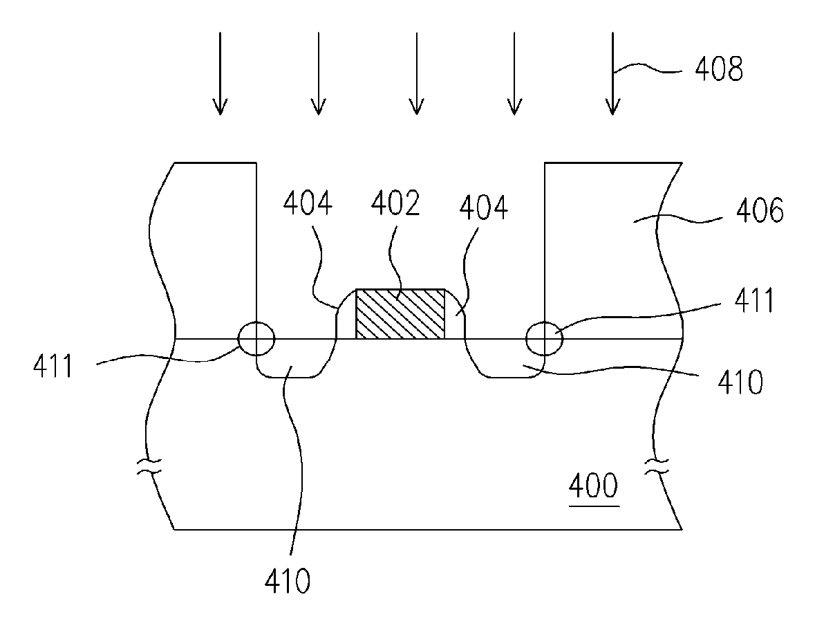
[0023]FIG. 4 is a cross-sectional view of a MOS transistor during the ion implantation process according to one preferred embodiment of this invention. The MOS transistor includes a gate 402 and spacers 404 formed on a substrate 400. The substrate 400 may further include other electronic components and will not be depicted in the figure. A conductive photoresist pattern 406 is formed over the substrate 400 and exposes a portion of the substrate 400. The material of the conductive photoresist pattern 406 includes at least a conductive resin, a solvent and a selectively photosensitive material. The conductive resin can be 3-hexylthiophene-3-thiophene-ethane methacrylate copolymer, for example. The so...


PUM


Abstract

In the plasma etching process of the integrated circuit, a portion of the charges from the plasma accumulates on the semiconductor device through the conductive portion of the integrated circuit so as to damage the device. The phenomenon mentioned above is so called antenna effect. In order to decreased the number of the accumulated charges caused by antenna effect and to alleviate the damage of the accumulated charges on the device, the conductive photoresist is used in the plasma etching process. The method for applying the conductive photoresist in the integrated circuit process is as same as the application method for using the well known standard photoresist.

Description

BACKGROUND OF THE INVENTION [0001] 1. Field of the Invention [0002] The present invention generally relates to a fabrication method for semiconductor devices, in particular, to a method for reducing positive charges accumulated on chips during ion implantation. [0003] 2. Description of Related Art [0004] The ion implantation process is in general applied to form doped regions in the semiconductor substrates. During the ion implantation process, the exposed substrate is implanted with desired dopants through the patterned photoresist layer. Usually, the dopants (i.e. ions) used in the ion implantation process carry positive charges. Hence, after implanting dopants to the substrate, positive charges are accumulated on the surface of the chip. [0005]FIG. 1 is a cross-sectional view of a MOS transistor during the ion implantation process. As shown in FIG. 1, the MOS transistor including a gate 102 and spacers 104 is formed on a substrate 100. The patterned photoresist layer 106 is used ...

Claims


Application Information

Patent Timeline
IPC IPC(8): H01L21/426
CPCH01L21/266H01L29/66272H01L21/8249
Inventor SHIH, HUI-SHENHUANG, KUAN-I
Owner UNITED MICROELECTRONICS CORP
Why Eureka
Try Eureka