Semiconductor integrated circuit for reducing leak current through MOS transistors

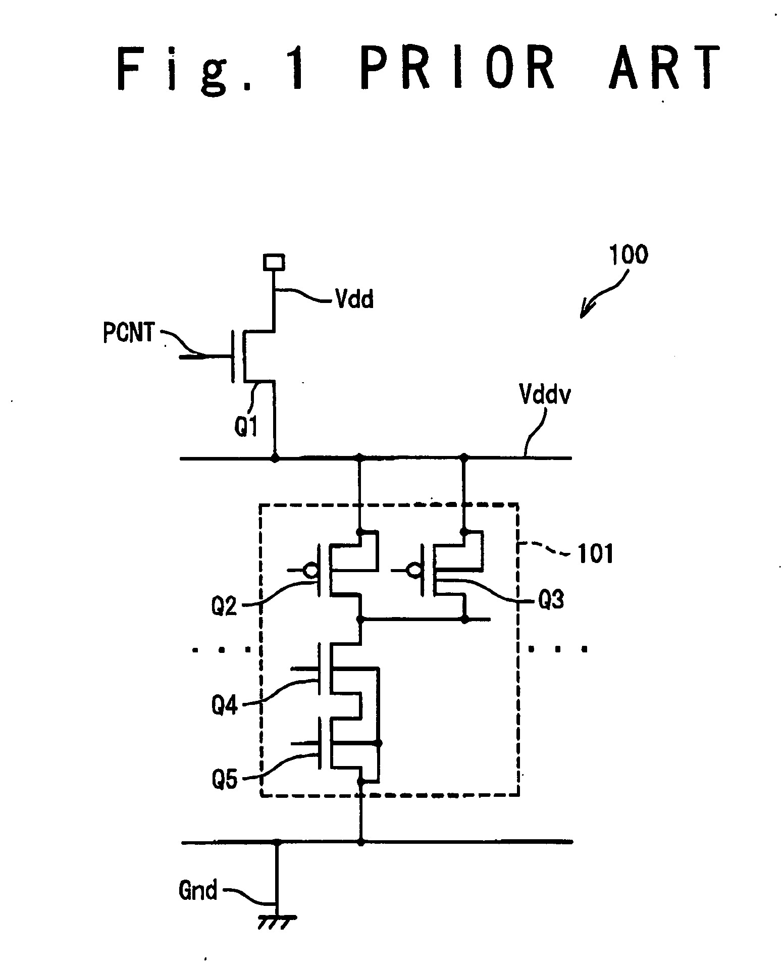
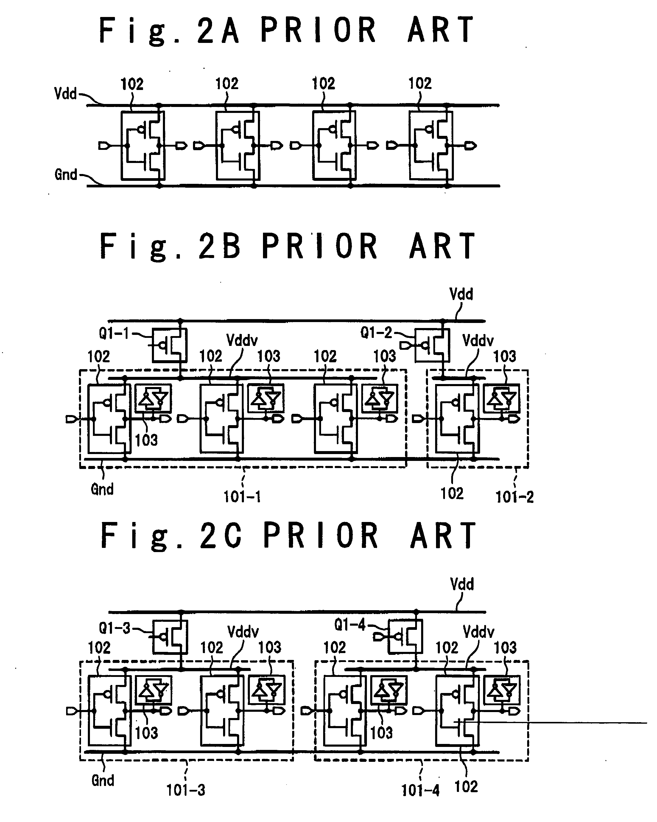
a technology of integrated circuits and mos transistors, which is applied in the direction of power consumption reduction, instruments, solid-state devices, etc., can solve the problems of increasing off-leak current, large percentage of total power consumption, and the proper sizing of sleep transistors requires a complicated circuit design process, so as to reduce rushing current and reduce rushing current.

Active Publication Date: 2007-03-29
RENESAS ELECTRONICS CORP
View PDF4 Cites 8 Cited by
  • Summary
  • Abstract
  • Description
  • Claims
  • Application Information

AI Technical Summary

Benefits of technology

[0012] Such arrangement allows sizing of the switch elements within the respective switch cells only on the basis of the maximum allowed current of the basic power supply lines. This eliminates the need for sizing the switch elements on the basis of the circuit structure within the power control region.
[0013] In a preferred embodiment, the switch transistors within the switch cells are turned on at different timings when the power control region is activated. This effectively reduces rushing currents when the power control region starts to be fed with the power supply voltage. The increase in the number of the switch cells is effective for reducing the rushing currents.

Problems solved by technology

One issue in the advance of the high-density integration of semiconductor devices is the increase in the off-leak current, which designates the current undesirably flowing through off-state MOS transistors.
In recent semiconductor devices, the off-leak current accounts for large percentages of total power consumption.
One issue of the MT-CMOS technology is proper transistor sizing of sleep transistors, such as the high-threshold NMOS transistor Q1 and PMOS transistors Q1-1 to Q1-4.
However, proper transistor sizing of the sleep transistors requires a complicated circuit design process.

Method used


Image

  • Semiconductor integrated circuit for reducing leak current through MOS transistors
  • Semiconductor integrated circuit for reducing leak current through MOS transistors
  • Semiconductor integrated circuit for reducing leak current through MOS transistors

Examples


first embodiment

(First Embodiment)

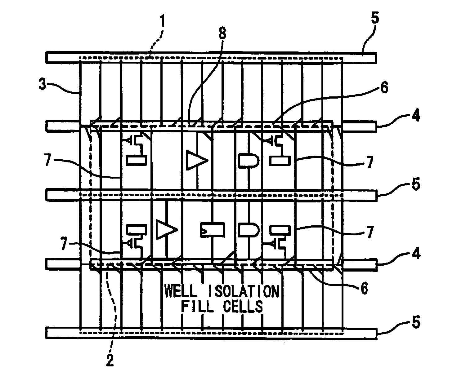
[0035]FIG. 3 is a plan view illustrating an exemplary configuration of a semiconductor device in a first embodiment. The semiconductor device in this embodiment is provided with a macro region 1 in which function cells 8 are arranged in rows and columns. The function cells 8 each incorporate a logic circuit. The macro region 1 is fed with power supply to operate the function cells 8.

[0036] The macro region 1 includes a power control region 2. The semiconductor device in this embodiment is designed so that the power supply to the power control region 2 is suspended to reduce power consumption, when the semiconductor device is placed into the standby mode. In the design procedure, the power control region 2 is defined in the floor planning. The power control region 2 includes a plurality of switch cells 7 each incorporating a switch transistor or sleep transistor. Details of the structure of the switch cells 7 will be described later.

[0037] The semiconductor device...

second embodiment

(Second Embodiment)

[0063] A description is made of a second embodiment of the present invention, with reference to FIGS. 10 to 16. It should be noted that the same numerals denote the same elements in the attached figures.

[0064]FIG. 14 is a plan view illustrating an exemplary structure of a semiconductor device in a second embodiment of the present invention. The structure of the semiconductor device in the second embodiment is almost similar to that in the second embodiment. The switch cells 7 and the function cells 8 are provided in the power control region 2, within the macro region 1.

[0065] one difference is that the first power supply lines 4 are distributed over the whole of the macro region 1, including the power control region 2 in the second embodiment; the first power supply lines 4 are positioned to overlap the power control region 2. The first power supply lines 4 and the ground lines 5 are arranged in parallel at constant intervals, and the second power supply lines 6...


PUM


Abstract

A semiconductor device is composed of: a power control region within which function cells are arranged; a basic power supply line overlapping said power control region, and positioned in a power supply interconnection layer; a virtual power supply line arranged in said power control region in a direction perpendicular to said basic power supply line, said function cells being connected to said virtual power supply line; a ground line arranged in said power control region in said direction perpendicular to said basic power supply line; a switch cell including a metal interconnection positioned in a metal interconnection layer different from said power supply interconnection layer, and a switch element electrically connected between said metal interconnection and said virtual power supply line; and a via contact connected between said basic power supply line and said metal interconnection. The switch cell is positioned within power control region. The switch element is positioned adjacent to said via contact within said switch cell. The metal interconnection is positioned between said virtual power supply line and said ground line within said switch cell.

Description

BACKGROUND OF THE INVENTION [0001] 1. Field of the Invention [0002] The present invention relates to semiconductor integrated circuit architecture for reducing undesirable off-leak currents through MOS transistors. [0003] 2. Description of the Related Art [0004] One issue in the advance of the high-density integration of semiconductor devices is the increase in the off-leak current, which designates the current undesirably flowing through off-state MOS transistors. In recent semiconductor devices, the off-leak current accounts for large percentages of total power consumption. Therefore, various techniques have been proposed for reducing the power consumption resulting from the off-leak current. [0005] One approach for reducing the off-leak current is the MT-CMOS (multi-threshold CMOS) technology. Japanese Laid-Open Patent Application No. JP-A 2004-186666 discloses a semiconductor device based on the MT-CMOS technology. FIG. 1 illustrates the structure of the disclosed semiconductor ...

Claims


Application Information

Patent Timeline
Patent Type & Authority Applications(United States)
IPC IPC(8): G06F17/50
CPCH03K19/0016H01L27/0203
Inventor KATOH, TETSUYA
Owner RENESAS ELECTRONICS CORP
Why Eureka
Try Eureka