Package board and semiconductor device

Inactive Publication Date: 2007-04-05
RENESAS ELECTRONICS CORP
View PDF3 Cites 4 Cited by
  • Summary
  • Abstract
  • Description
  • Claims
  • Application Information

AI Technical Summary

Benefits of technology

[0016] According to the present invention, the semiconductor chip is mounted on the package board in which the girdle-shaped insulating film is provided along the side of the bump formation region and the opening section is provided within the region on a side of the girdle-shaped insulating film. It is therefore possible to obtain the semiconductor device having excellent connection reliability.
[0017] According to the present invention, the girdle-shaped insulating film is provided around the region and along the side of the bump formation region opposite to t

Problems solved by technology

There are problems with the conventional technique in the following points.
Therefore, crack and/or exfoliation originating from the void may occur due to heat stress during an assembly process, an envir

Method used


Image

  • Package board and semiconductor device
  • Package board and semiconductor device
  • Package board and semiconductor device

Examples


Example

[0024] The invention will be now described herein with reference to illustrative embodiments. Those skilled in the art will recognize that many alternative embodiments can be accomplished using the teachings of the present invention and that the invention is not limited to the embodiments illustrated for explanatory purposed.

[0025] The embodiments of the present invention will be described with reference to the attached drawings. In the respective drawings, the same numerals are given to the same elements, and redundant explanation will be omitted suitably.

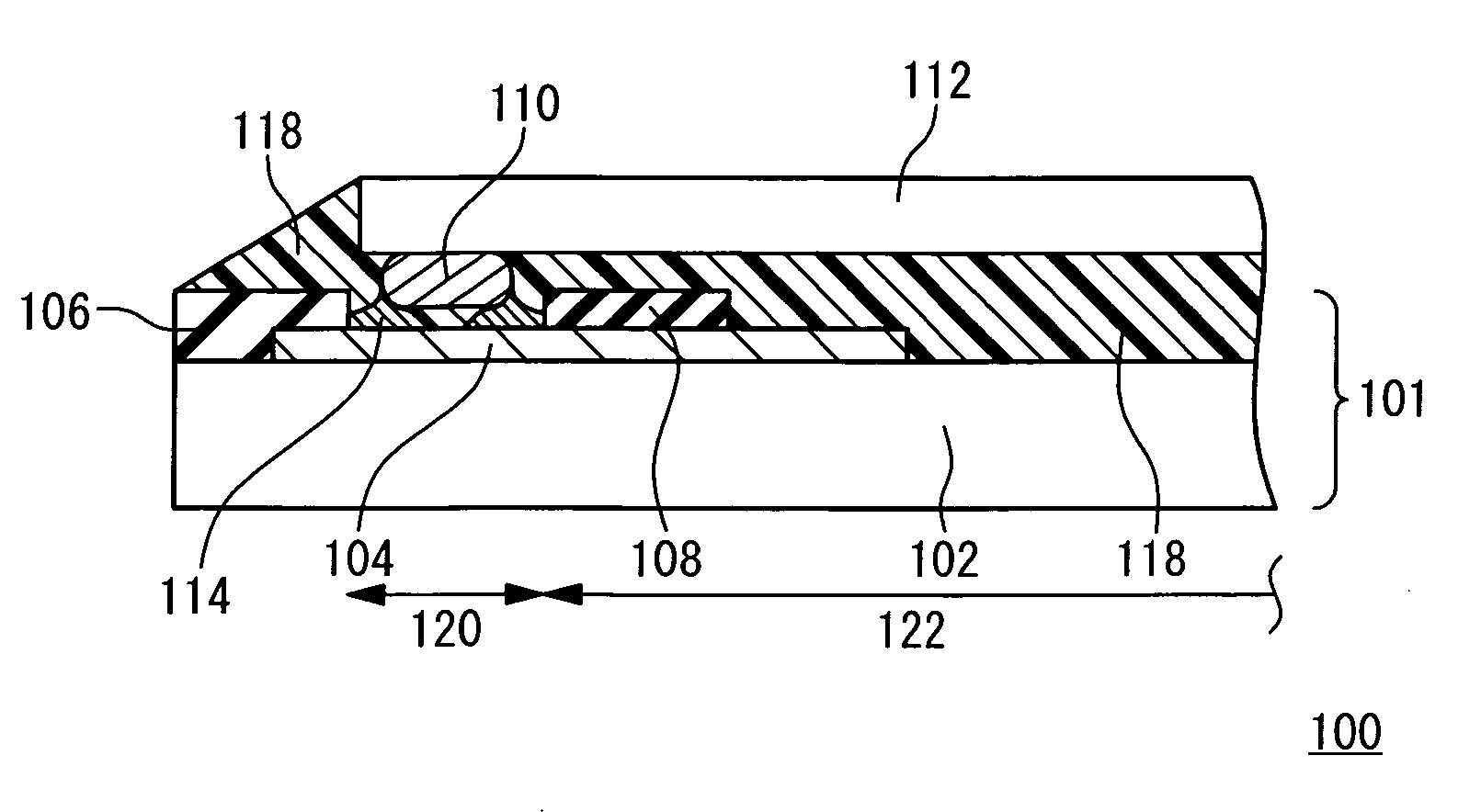
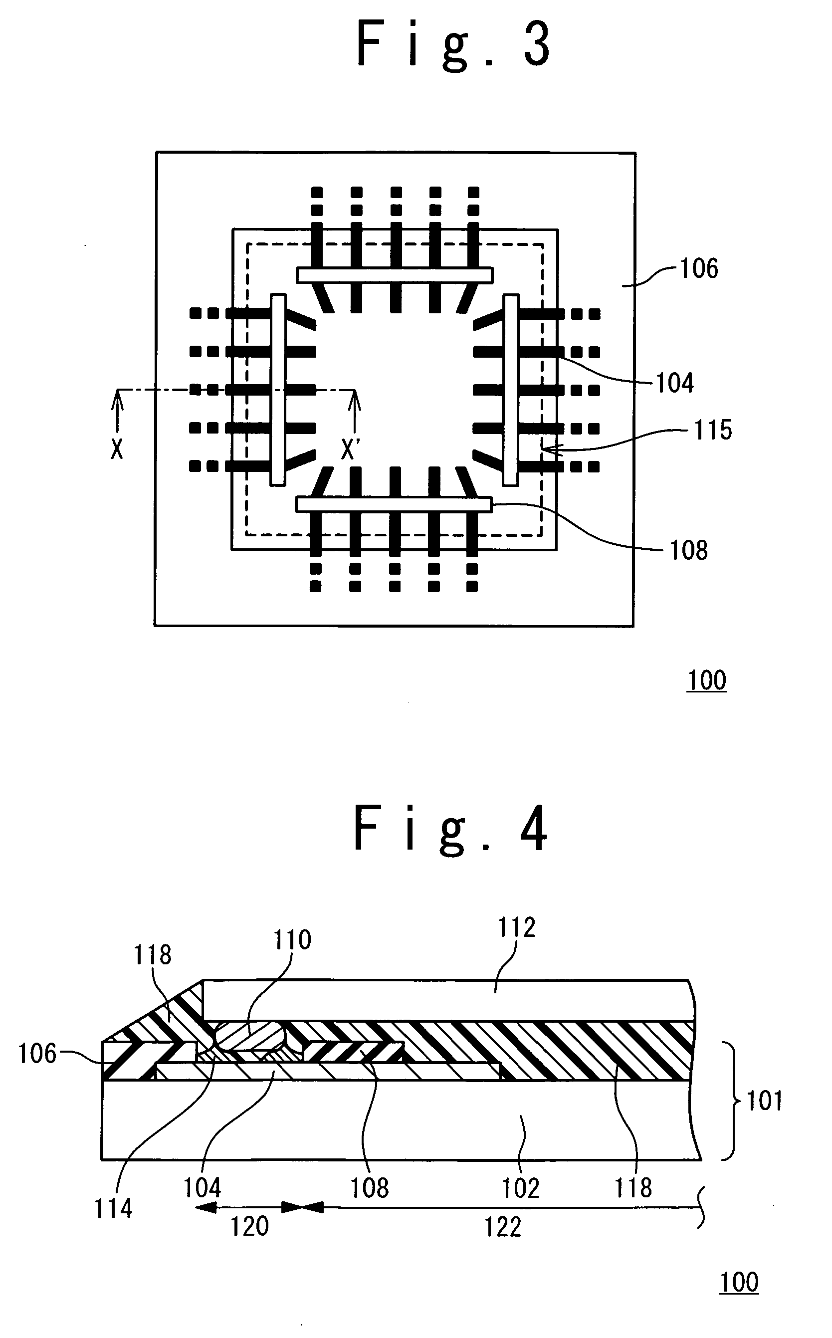
[0026] A semiconductor device 100 shown in FIGS. 3 and 4 has a board (a package board 101) for flip-flop packaging and an element (a semiconductor chip 112). The element (the semiconductor chip 112) is mounted on one surface of the board (the package board 101) in facedown manner and has a flip-chip connection to the board (the package board 101). The board (the package board 101) has: an interconnection 104 provided on the one ...


PUM


Abstract

A package board for flip-chip packaging on whose one surface an element is mounted in a facedown manner is provided. The package board has: an interconnection provided on the one surface; a bump formation region in which a bump electrically connecting the interconnection with an electrode pad of the element is provided; and an insulating film covering a part of the one surface outside of the bump formation region. The insulating film includes a girdle-shaped insulating film that is provided around a region and along a side of the bump formation region opposite to an edge of the package board. The insulating film further has an opening section formed within the region.

Description

BACKGROUND OF THE INVENTION [0001] 1. Field of the Invention [0002] The present invention relates to a package board and a semiconductor device using the package board. [0003] 2. Description of the Related Art [0004] In recent years, a demand on a small-size, thin, high-speed semiconductor device is increasing. In order to meet such a demand, a flip-chip connection technique is introduced in which a semiconductor chip is directly mounted on a package board in a facedown manner. According to a conventional wire bonding technique, a semiconductor chip has been connected to a gold bonding wire. On the other hand, according to the flip-chip connection technique, gold stud bumps and the like are formed on electrode pads of the semiconductor chip, and thereby the flip-chip connection between the semiconductor chip and the package board is achieved. The flip-chip connection can be achieved at relatively low cost. [0005] There are several methods for electrically connecting a semiconductor ...

Claims


Application Information

Patent Timeline
IPC IPC(8): H01L23/48
CPCH01L21/563H01L2224/73203H01L2924/01078H01L2924/01079H01L24/16H01L2224/16225H01L2224/32225H01L2224/73204H01L2924/00H01L2924/01029H01L2224/10175H01L2924/14
Inventor MAEDA, MASATO
Owner RENESAS ELECTRONICS CORP
Why Eureka
Try Eureka