Connection substrate, multi-layer wiring board using the connection substrate, substrate for semiconductor package, and methods for manufacturing them

Inactive Publication Date: 2006-07-27
HITACHI CHEM CO LTD
View PDF8 Cites 10 Cited by
  • Summary
  • Abstract
  • Description
  • Claims
  • Application Information

AI Technical Summary

Benefits of technology

[0011] The present invention was developed in the light of the above-described drawbacks and an object of the present invention is to provide a connection board that 1) inter-layer connection can be performed only at required positions without performing a drilling step, 2) a strong filled via structure can be formed, 3) a fine wiring circui

Problems solved by technology

According to this method, however, since holes are formed at all layers, a wiring capacity is limited.
According to the laser method of the prior arts, a selection range of insulating materials is large, although drilling can be performed not only for adjacent layers but also for adjacent layers and next adjacent layers, there arise problems in that a de-smear treatment is required for removing foreign matters of resin diffused by laser irradiation and a working cost is increased in proportion to the number of holes.
Nevertheless, there arise problems in that the resolution of inter-layer insulating material and heat resistance, moreover strength of adhesion between a circuit and an insulating resin composition layer cannot be accomplished at the same time.
Further, since the bump is

Method used


Image

  • Connection substrate, multi-layer wiring board using the connection substrate, substrate for semiconductor package, and methods for manufacturing them
  • Connection substrate, multi-layer wiring board using the connection substrate, substrate for semiconductor package, and methods for manufacturing them
  • Connection substrate, multi-layer wiring board using the connection substrate, substrate for semiconductor package, and methods for manufacturing them

Examples


Example

EXAMPLE 1

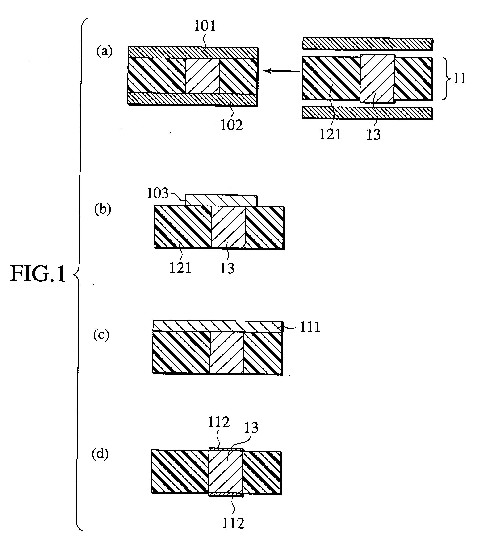
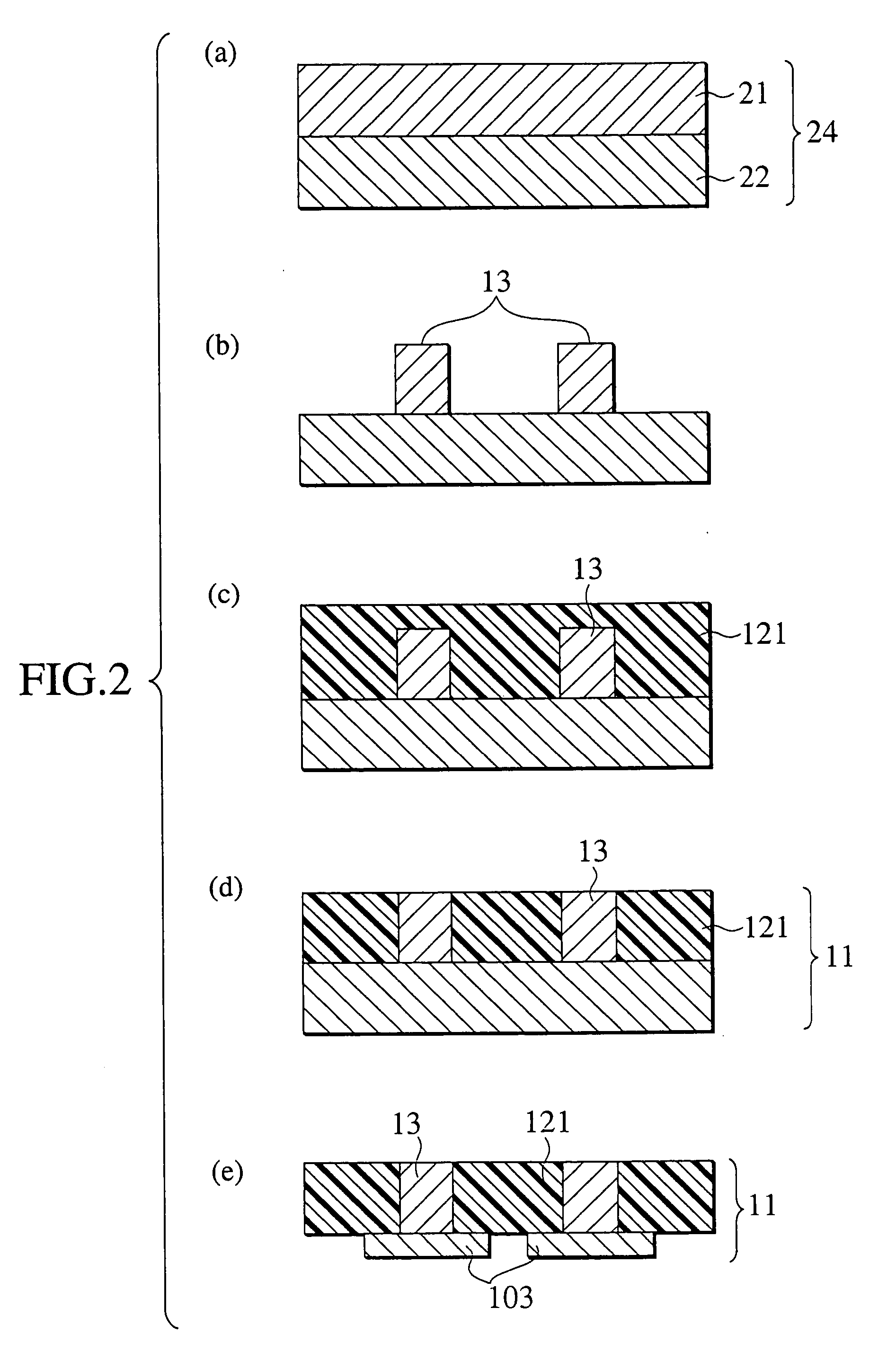
[0089] As shown in FIG. 4(a), a composite metallic layer 4 formed of 70 μm of first metallic layer 41 made of copper, 0.2 μm of third metallic layer 43 made of nickel and 35 μm of second metallic layer 42 made of copper was prepared. As shown in FIG. 4(b), a resist NCP225 or NIT225 (trade name manufactured by Nichigo-Morton Co., Ltd.) serving as an etching resist 44 was laminated on a surface of the first metallic layer 41 under conditions such as 110° C. of roll temperature and 0.6 m / min. of roll speed, formed under exposure conditions such as 80 mJ / cm2 of accumulated exposure amount, developed with sodium carbonate solution and subjected to post-exposure in order to ensure close contact of the resist. A rear surface is completely protected by laminating the etching resist 44 and exposing it on the same conditions as the above.

[0090] Then, an alkaline etching A process solution (trade name manufactured by Meltex Inc.) serving as an etchant which did not erode nickel was ...

Example

EXAMPLE 2

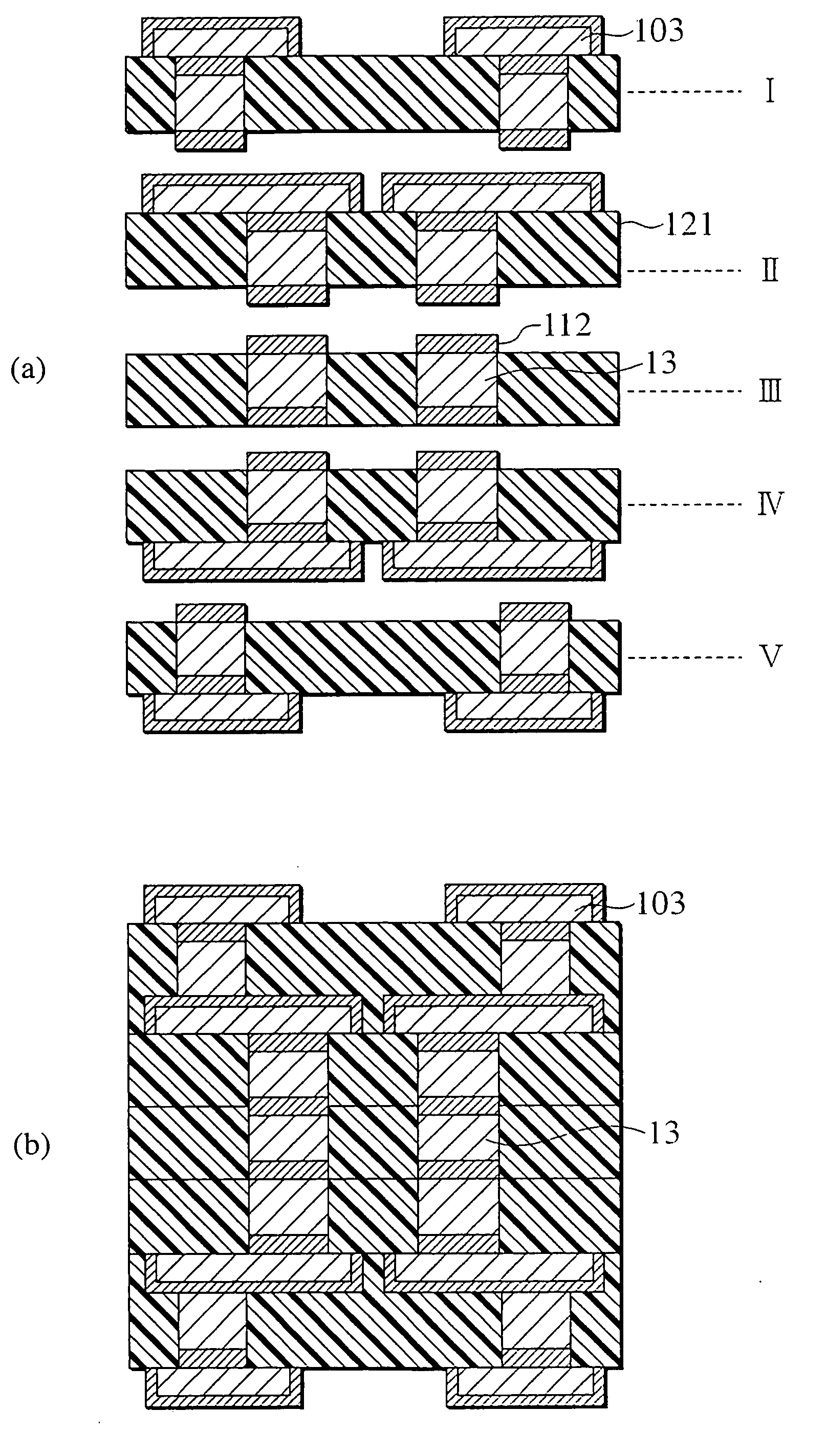
[0095] Electroless nickel plating, electroless palladium plating and electroless gold plating were successively performed upon surfaces of various connection boards obtained in Example 1. Then, the connection boards subjected to plating treatment were aligned as shown in FIG. 5(a) by guide pins and laminated at a time by pressing again at 333° C. In this way, a multi-layer wiring board shown in FIG. 5(b) was produced and its conductive connection by alloy of gold and gold was confirmed. At that time, an insulating resin composition between the connection boards was melted again and adhered with each other. When either of substitution type electroless tin plating and reduction type electroless tin plating was utilized for plating of connection boards, a multi-layer wiring board could be produced. Electroless nickel plating, electroless palladium plating and electroless gold plating were performed upon a connection board at an outermost layer and electroless tin plating was ...

Example

EXAMPLE 3

[0096] A substrate for semiconductor package and a semiconductor package were produced by using the connection board of FIG. 4(f) obtained in Example 1. Firstly, in order to form a fine circuit on a metallic layer 111 by etching, half etching for reducing a thickness of the metallic layer 111 to 18 μm was performed by spraying an etchant, prepared in such a manner that 100 g / L of aqueous hydrogen peroxide solution, sulfic acid and copper sulfate were mixed with each other and a resultant solution was adjusted so as to obtain 30 g / L of density of copper, on both sides of FIG. 6(a) at 35° C. of temperature of solution (FIG. 6(b)) At this time, since the thickness of ends of connection conductor is reduced, soldering balls are easily placed on such thinned end portions.

[0097] Then, as shown in FIG. 6(c), the conductor circuit 103 was formed by selectively removing the metallic layer 111 by etching. As shown in FIG. 6(d), electroless nickel plating, electroless palladium plat...


PUM

PropertyMeasurementUnit
Timeaaaaaaaaaa
Thicknessaaaaaaaaaa
Electrical conductoraaaaaaaaaa

Abstract

The present invention provides a connection board that is formed by an insulating resin composition layer made of one layer or two or more layers and a connection conductor that is formed so as to pass through the insulating resin composition layer in its thickness direction at a position where a conductor circuit is connected, and a multi-layer wiring board, a substrate for semiconductor package and a semiconductor package using the connection board, and methods for manufacturing them.

Description

FIELD OF THE INVENTION [0001] The present invention relates to a connection board, and a multi-layer wiring board, a substrate for semiconductor package, a semiconductor package using the connection board, and manufacturing method of them. BACKGROUND OF THE INVENTION [0002] Recently, the social environment surrounding us has been changing greatly according to an improvement in information communication network. Among such changes, the growth of mobile equipments is included. Their markets are being extended according to compactness and high functionality thereof. For this reason, further compactness of semiconductor package and multi-layer wiring substrate which is capable of mounting the package with high density are required. Further, inter-layer connection enabling high density wiring, i.e., technique for forming multiple layers with high density becomes important. [0003] A through-hole connection that drilling and plating processes are combined is mainly provided as the method o...

Claims


Application Information

Patent Timeline
IPC IPC(8): H05K1/03H05K1/09H05K1/11H01L23/498H05K3/40H05K3/46
CPCH01L21/4857H01L21/486H01L23/3128H01L23/49822H01L23/49827H01L24/45H01L24/48H01L24/73H01L2224/32225H01L2224/45144H01L2224/48091H01L2224/48227H01L2224/73265H01L2224/92247H01L2924/01046H01L2924/01078H01L2924/01079H01L2924/01327H01L2924/15183H01L2924/15311H01L2924/181H05K3/0097H05K3/06H05K3/244H05K3/4038H05K3/4617H05K3/4623H05K3/4632H05K3/4647H05K2201/0141H05K2201/0195H05K2201/0355H05K2201/0361H05K2201/096H05K2201/10378H05K2203/0152H05K2203/0156H05K2203/0384H05K2203/0733H05K2203/1536Y10T29/49126Y10T29/4913Y10T29/49147Y10T29/49165H01L2924/00014H01L2924/00H01L2924/00012H05K1/11H05K3/46
Inventor NAKAMURA, HIDEHIRONAKASO, AKISHIARIKE, SHIGEHARUINOUE, FUMIOENOMOTO, TETSDUYAMORIIKE, NORIOHIROKI, KOUSUKE
Owner HITACHI CHEM CO LTD
Why Eureka
Try Eureka