Method of producing multilayer printed wiring board and photosensitive dry film used therefor

Active Publication Date: 2007-05-03
IBIDEN CO LTD
View PDF1 Cites 17 Cited by
  • Summary
  • Abstract
  • Description
  • Claims
  • Application Information

AI Technical Summary

Benefits of technology

[0012] According to the production method of multilayer printed wiring board and the photosensitive dry film used therein of the invention, the compatibility between the thin-film conductor layer and the photosensitive dry film is improved and the adhesion force between the thin-film conductor layer and the photosensitive dry film is strengthened, so that when the photosensitive dry film is attached to t

Problems solved by technology

However, when the photosensitive dry film is directly attached onto the interlaminar resin insulating layer having the thin-film conductor layer on its surface, a part of the surface of the thin-film conductor layer may be modified by the oxidation or the like, and hence the properties of the surface of the thin-film conductor layer becomes not uniform.
Such a problem is frequently caused in case of a conductor circui

Method used


Image

  • Method of producing multilayer printed wiring board and photosensitive dry film used therefor
  • Method of producing multilayer printed wiring board and photosensitive dry film used therefor
  • Method of producing multilayer printed wiring board and photosensitive dry film used therefor

Examples


example 1

[0063] The invention will be described in detail with reference to the following examples below.

[0064] (A) Preparation of Scale-Like Particle-Containing Kneaded Mass

[0065] To a mixed solvent of 20 g of methylethyl ketone (hereinafter referred to as “MEK”) and 80 g of xylene is added 15 g of scale-like particles (trade name: Esben C, made by Houjunn Corp., aspect ratio in dispersion: 500 or less than 500, crystal size: 0.5 μm or less than 0.5 μm), which are kneaded through three rollers to form a scale-like particle-containing kneaded mass.

[0066] (B) Preparation of Epoxy-Containing Solution

[0067] To a mixed solvent of 6.8 g of MEK and 27.2 g of xylene is added and mixed 85 g of solid epoxy resin (trade name: Epicoat 1007, made by Japan Epoxy Resin Co., Ltd.) to form an epoxy containing solution.

[0068] (C) Preparation of Resin Film for Interlaminar Resin Insulating Layer

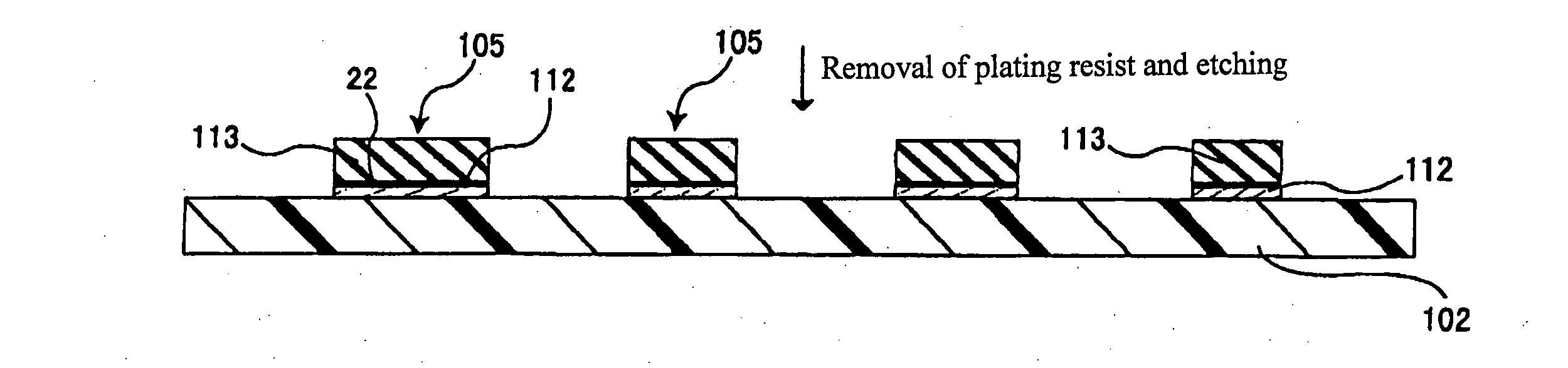
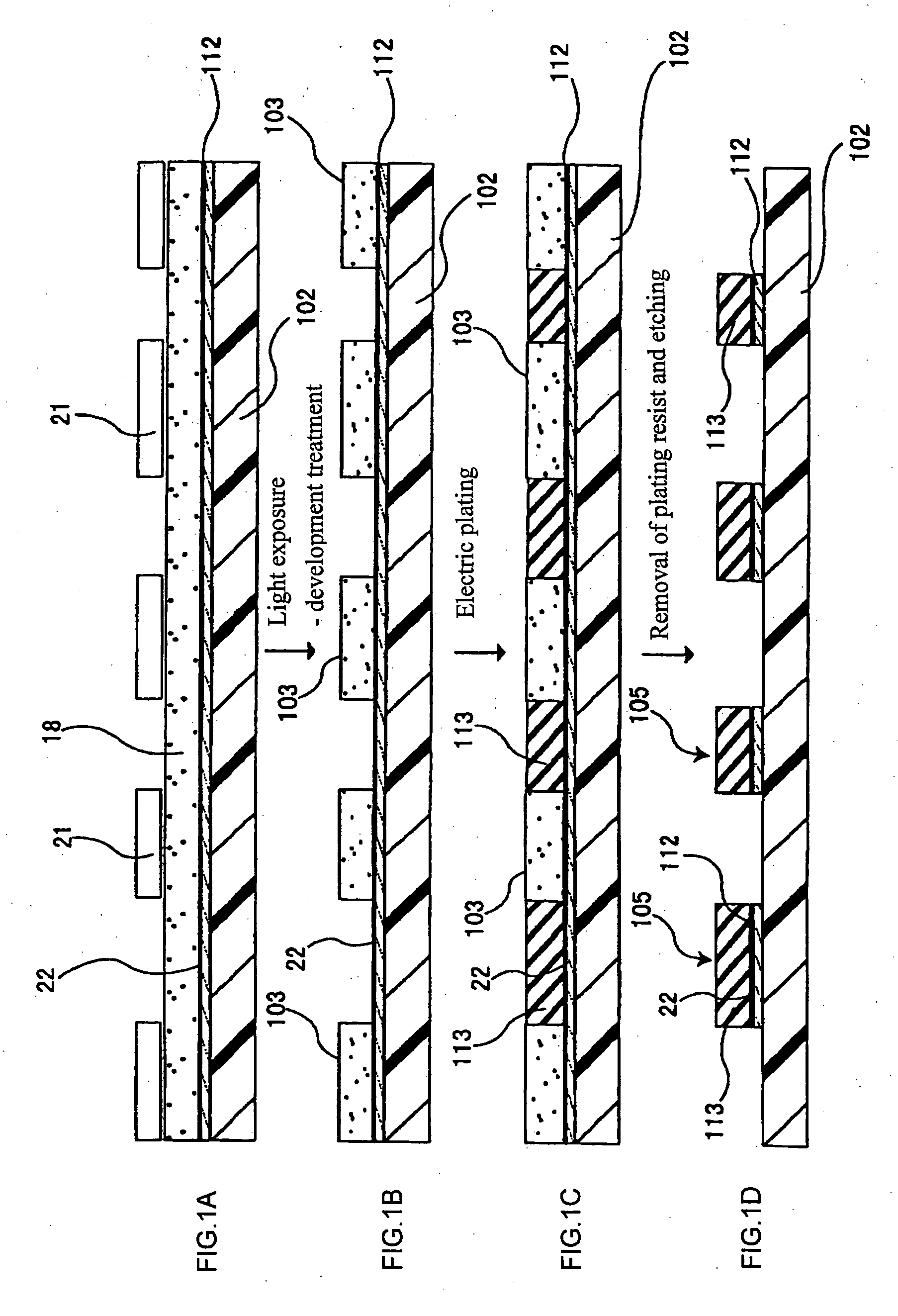
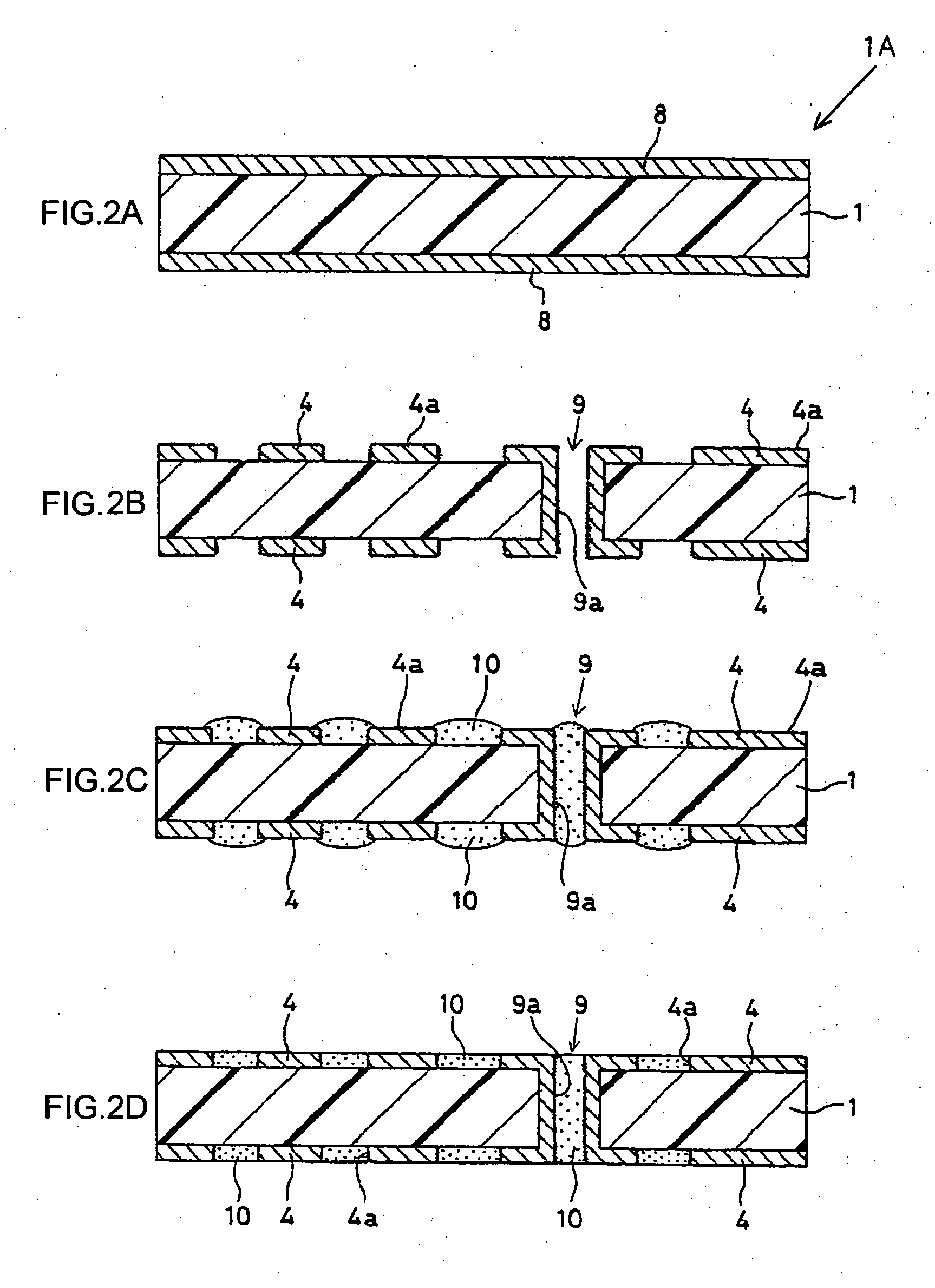
[0069] The scale-like particle-containing kneaded mass prepared in the item (A), the epoxy containing solution...

example 2-5

[0097] Multilayer printed wiring boards are prepared in the same manner as described above except that the concentration of the solution containing 5-aminotetrazole is 1 wt %, 3 wt %, 8 wt % or 10 wt % in the step (E) of preparing the dry film.

example 6

[0098] A multilayer printed wiring board is prepared in the same manner as in Example 1 except that 5-amino-1,2,3-methyltetrazole having a concentration of 3 wt % is used instead of 5-aminotetrazole having a concentration of 0.5 wt % in the step (E) of preparing the dry film.


PUM

PropertyMeasurementUnit
Fractionaaaaaaaaaa
Fractionaaaaaaaaaa
Fractionaaaaaaaaaa

Abstract

A method of producing a multilayer printed wiring board by attaching a photosensitive dry film onto an interlaminar resin insulating layer having a thin-film conductor layer and conducting a light exposure and development to form a plating resist and then forming a conductor circuit on a portion not forming the plating resist, characterized in that the photosensitive dry film has a nitrogen-containing heterocyclic compound layer on its either surface. A photosensitive dry film capable of improving the compatibility between thin-film conductor layer and photosensitive dry film to strengthen the adhesion force and to prevent the occurrence of floating or the like in the photosensitive dry film as well as a method of producing a multilayer printed wiring board using such a dry film.

Description

TECHNICAL FIELD [0001] This invention relates to a method of producing a multilayer printed wiring board and a photosensitive dry film used for this production method. RELATED ART [0002] The multilayer printed wiring board called as a build-up multilayered printed wiring board is a package corresponding to the speeding-up and high integration of IC chips and is characterized in points that the electric resistance and dielectric constant are small and the weight reduction is excellent. The multilayer printed wiring board is produced by a semi-additive method or the like wherein conductor circuits of copper or the like and interlaminar resin insulating layers are alternately laminated on a resin substrate reinforced with a glass cloth or the like of about 0.6-1.5 mm called as a core. [0003] Heretofore, the multilayer printed wiring board has been produced through the following steps disclosed in JP-A-H09-130050. That is, the multilayer printed wiring board is produced by 1) forming t...

Claims


Application Information

Patent Timeline
IPC IPC(8): B32B37/00
CPCH05K3/108Y10T29/49117H05K2203/124H05K3/389Y10T428/31504
Inventor TSUDA, AKIYOSHI
Owner IBIDEN CO LTD
Why Eureka
Try Eureka