Magnetoresistive effect element and magnetic memory device

a magnetic memory device and effect element technology, applied in information storage, static storage, digital storage, etc., can solve the problems of increased electric power consumption, increased write current, and defective write, and achieve good symmetry, large resistance change, and reduced magnetization reversing current

Inactive Publication Date: 2007-04-05
FUJITSU LTD
View PDF4 Cites 71 Cited by
  • Summary
  • Abstract
  • Description
  • Claims
  • Application Information

AI Technical Summary

Benefits of technology

[0018] An object of the present invention is to provide a magnetoresistive effect element using spin transfer torque switching mechanism which can decrease the magnetization reversing current, can realize the resistance-current hysteresis characteristic having good symmetry with the shift suppressed, and can realize large resistance changes, and a magnetic memory device using the magnetoresistive effect element.
[0019] According to one aspect of the present invention, there is provided a magnetoresistive effect element comprising: a first pinned magnetic layer having a multilayered synthetic antiferromagnet (SAF) structure formed of a plurality of ferromagnetic layers stacked with a nonmagnetic layer formed therebetween; a first nonmagnetic spacer layer formed on the first pinned magnetic layer; a free magnetic layer formed on the first nonmagnetic spacer layer and including an odd number of ferromagnetic layers; a second nonmagnetic spacer layer formed on the free magnetic layer; and a second pinned magnetic layer formed on the second nonmagnetic spacer layer and having a multilayered SAF structure formed of a plurality of ferromagnetic layers stacked with a nonmagnetic layer formed therebetween, a magnetization direction of the ferromagnetic layer of the first pinned magnetic layer, which is nearest the free magnetic layer, and a magnetization direction of the ferromagnetic layer of the second pinned magnetic layer, which is nearest the free magnetic layer, being opposite to each other.
[0020] According to another aspect of the present invention, there is provided a magnetoresistive effect element comprising: a first pinned magnetic layer having a multilayered SAF structure formed of a plurality of ferromagnetic layers stacked with a nonmagnetic layer formed therebetween; a first nonmagnetic spacer layer formed on the first pinned magnetic layer; a free magnetic layer formed on the first nonmagnetic spacer layer and including an even number of ferromagnetic layers; a second nonmagnetic spacer layer formed on the free magnetic layer; and a second pinned magnetic layer formed on the second nonmagnetic spacer layer and having a multilayered SAF structure formed of a plurality of ferromagnetic layers stacked with a nonmagnetic layer formed therebetween, a magnetization direction of the ferromagnetic layer of

Problems solved by technology

Accordingly, when the write current is small, defective write takes place.
Thus, as the integration increases, the write current is increased, and electric power consumption is increased.
937-948 (Non-Patent Reference 1) anticipates that when the memory cell size is reduced to about 100 nm so as to satisfy large capacities exceeding gigabits, the conventional current magnetic filed write method drastically increases the write current, and actually the write will be difficult.
The MRAM with selective transistors connected to must include write word lines in addition to the bit lines and the word lines, which complicates the device structure and the fabrication process.
This switch from parallel to anti-parallel has poor spin transfer effici

Method used


Image

  • Magnetoresistive effect element and magnetic memory device
  • Magnetoresistive effect element and magnetic memory device
  • Magnetoresistive effect element and magnetic memory device

Examples


first embodiment

A FIRST EMBODIMENT

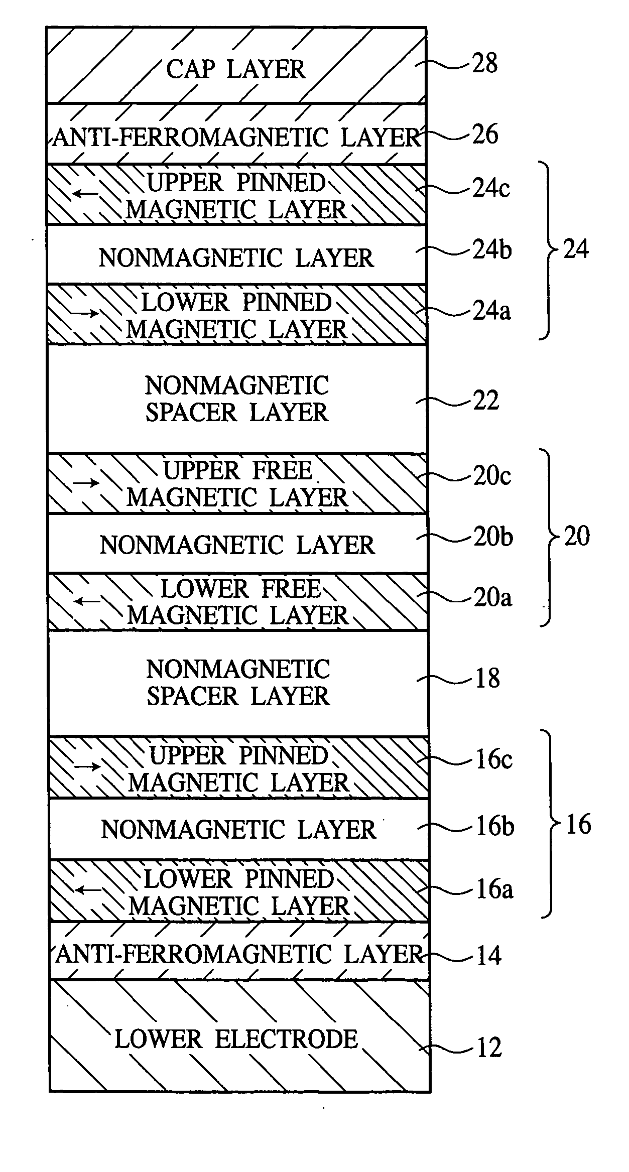
[0075] The magnetoresistive effect element and the method for fabricating the same according to a first embodiment of the present invention will be explained with reference to FIGS. 4, 5, 6A-6B, 7A-7B, 8A-8B and 9A-9B. FIG. 4 is a diagrammatic sectional view showing a structure of the magnetoresistive effect element according to the present embodiment. FIG. 5 is a graph of the resistance-current hysteresis characteristic of the magnetoresistive effect element according to the present embodiment. FIGS. 6A-6B, 7A-7B, 8A-8B and 9A-9B are sectional views of the magnetoresistive effect element according to the present embodiment in the steps of the method for fabricating the same, which show the method.

[0076] First, the structure of the magnetoresistive effect element according to the present embodiment will be explained with reference to FIG. 4.

[0077] As shown in FIG. 4, an inter-layer insulating film 30 is formed on a silicon substrate 10. An interconnection trench ...

second embodiment

A SECOND EMBODIMENT

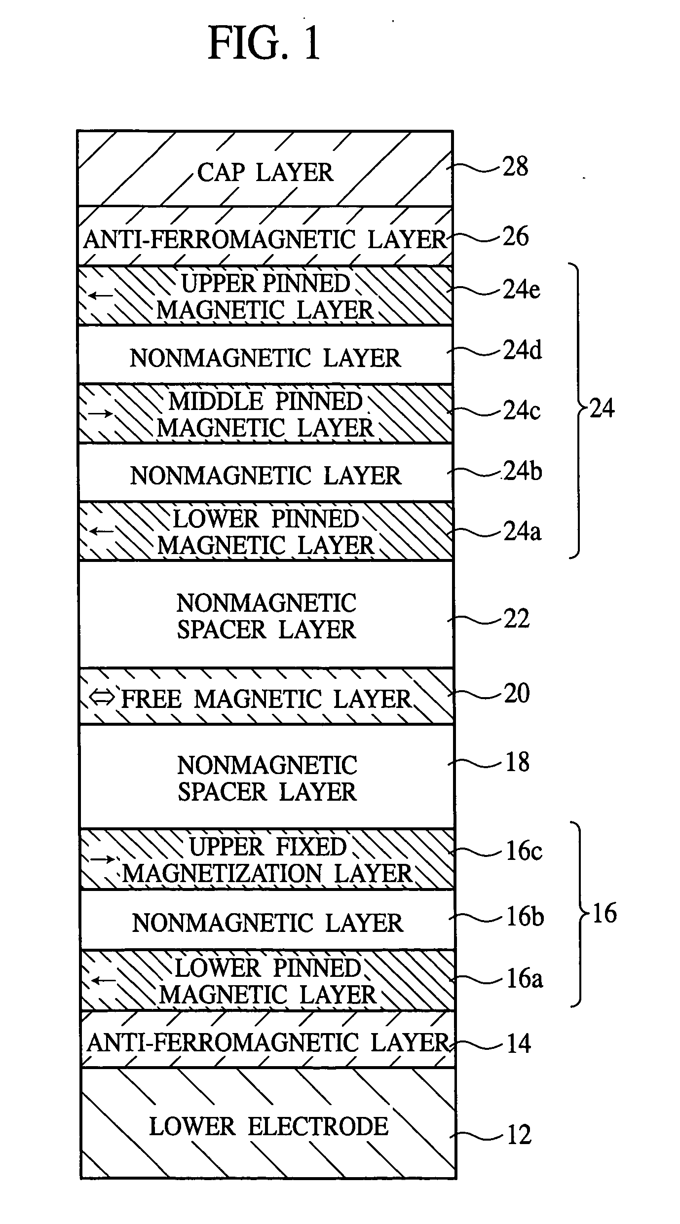
[0132] The magnetoresistive effect element and the method for fabricating the same according to a second embodiment of the present invention will be explained with reference to FIGS. 10, 11A-11B and 12A-12B. FIG. 10 is a diagrammatic sectional view showing a structure of the magnetoresistive effect element according to the present embodiment. FIGS. 11A-11B and 12A-12B are sectional views of the magnetoresistive effect element according to the present embodiment in the steps of the method for fabricating the same, which show the method. The same members of the present embodiment as those of the magnetoresistive effect element and method for fabricating the same according to the first embodiment are represented by the same reference numbers not to repeat or to simplify their explanation.

[0133] First, the structure of the magnetoresistive effect element according to the present embodiment will be explained with reference to FIG. 10.

[0134] As shown, a lower electrod...

third embodiment

A THIRD EMBODIMENT

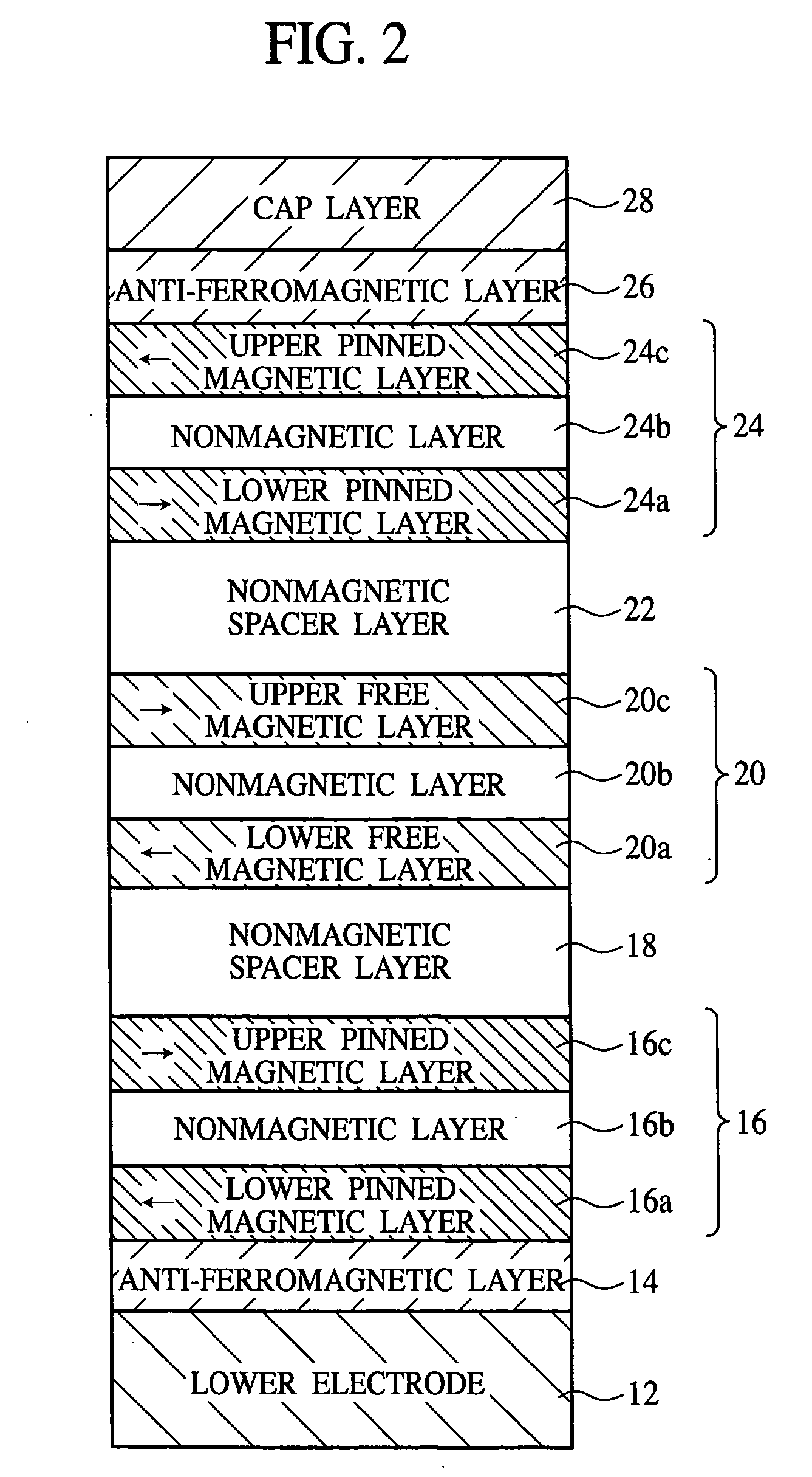
[0172] The magnetic memory device and the method for fabricating the same according to a third embodiment of the present invention will be explained with reference to FIGS. 13, 14A-14C, 15A-15B and 16A-16B. FIG. 13 is a diagrammatic sectional view showing a structure of the magnetic memory device according to the present embodiment. FIGS. 14A-14C, 15A-15B and 16A-16B are sectional views of the magnetic memory device according to the present embodiment in the steps of the method for fabricating the same, which show the method. The same members of the present embodiment as those of the magnetoresistive effect element and the method for fabricating the same according to the first embodiment are represented by the same reference numbers not to repeat or to simplify their explanation.

[0173] First, the structure of the magnetic memory device according to the present embodiment will be explained with reference to FIG. 13. The magnetic memory device according to the prese...


PUM


Abstract

The magnetoresistive effect element comprises a pinned magnetic layer 16 having a multilayered synthetic antiferromagnet (SAF) structure, a nonmagnetic spacer layer 18 formed on the pinned magnetic layer 16, a free magnetic layer 20 formed on the nonmagnetic spacer layer 18 and formed of a single ferromagnetic layer, a nonmagnetic spacer layer 22 formed on the free magnetic layer 20, and a pinned magnetic layer 24 of a multilayered SAF structure formed on the nonmagnetic spacer layer 22, wherein a magnetization direction of the ferromagnetic layer 16c of the pinned magnetic layer 16, which is nearest the free magnetic layer 20, and a magnetization direction of the ferromagnetic layer 24a of the pinned magnetic layer 24, which is nearest the free magnetic layer 20, are opposite to each other.

Description

CROSS-REFERENCE TO RELATED APPLICATIONS [0001] This application is based upon and claims the benefit of priority from the prior Japanese Patent Application No. 2005-269896, filed on Sep. 16, 2005, the entire contents of which are incorporated herein by reference. BACKGROUND OF THE INVENTION [0002] The present invention relates to a magnetoresistive effect element and a magnetic memory device, more specifically, a magnetoresistive effect element using spin transfer torque switching (spin transfer magnetization switching) mechanism, and a magnetic memory device using the magnetoresistive effect element. [0003] Recently, as a rewritable non-volatile memory, a magnetic random access memory (hereinafter called an MRAM) including magnetoresistive effect elements arranged in a matrix is noted. The MRAM memorizes information by using combinations of magnetization directions of two magnetic layers and reads memorized information by detecting resistance changes (i.e., current changes or volta...

Claims


Application Information

Patent Timeline
IPC IPC(8): G11C11/00
CPCG11C11/16H10B61/22H10N50/10
Inventor ASHIDA, HIROSHISATO, MASASHIGEUMEHARA, SHINJIROKOBAYASHI, KAZUO
Owner FUJITSU LTD
Why Eureka
Try Eureka