Production method of semiconductor chip

Active Publication Date: 2007-04-05
3M INNOVATIVE PROPERTIES CO
View PDF17 Cites 50 Cited by
  • Summary
  • Abstract
  • Description
  • Claims
  • Application Information

AI Technical Summary

Benefits of technology

[0006] Accordingly, an object of the present invention is to provide a method for producing a semiconductor chip, comprising

Problems solved by technology

Usually, in conventional techniques of performing the back-surface grinding and conveyance while holding the wafer only by a backgrinding protective tape, thinning can be accomplished in practice only to a thickness of about 150 μm because of problems such that the wafer with the protective tape is warped after grinding or the thickness at the grinding is low in the uniformity.
Particularly, in obtaining chips from a semiconductor wafer thinned to an extremely small thickness of 50 μm or less, a low yield in the dicing process becomes a

Method used


Image

  • Production method of semiconductor chip
  • Production method of semiconductor chip
  • Production method of semiconductor chip

Examples


example 1

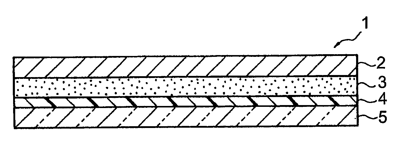
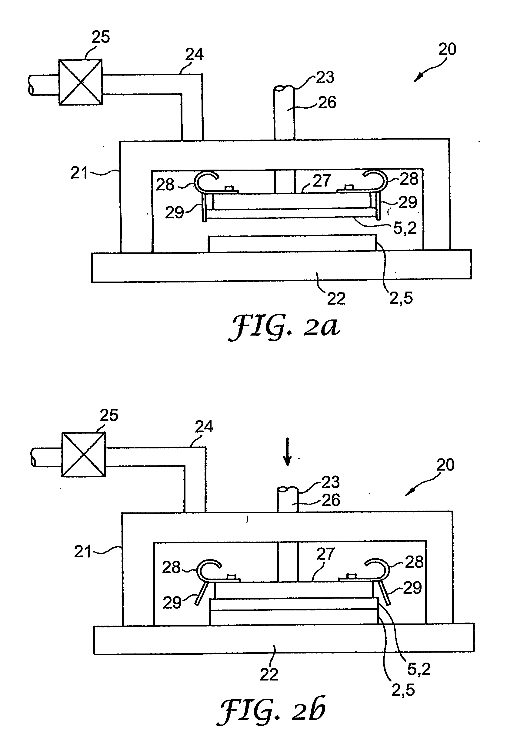
[0077] A glass substrate of 204 mm (diameter)×1.0 mm (thickness) was used as the light-transmitting support, and a silicon wafer of 200 mm (diameter)×750 μm (thickness) was used as the semiconductor wafer. A 10% solution (in propylene glycol methylether acetate solvent) of a photothermal conversion layer precursor having the composition shown in Table 1 below was coated on the glass substrate by spin coating. This was dried by heating and then cured by 1500 mJ / cm2 of ultraviolet (UV) irradiation to form a photothermal conversion layer on the support. On the other hand, an adhesive layer precursor having the composition shown in Table 2 below was coated on the wafer similarly by spin coating. The glass substrate and the wafer were laminated to each other in a vacuum adhesion apparatus shown in FIG. 2 and thereon, 1500 mJ / cm2 of UV was irradiated to cure the adhesive layer precursor, thereby obtaining a laminated body. This laminated body had a configuration of glass substrate / phototh...

example 2

[0084] A test was performed in the same manner as in Example 1 except that the composition of adhesive was changed as shown in Table 3 below and after curing the adhesive layer, the laminated body was placed in an oven at 120° C. for 3 minutes. The storage modulus at 25° C. of the adhesive layer after curing was 1.5×10⁸ Pa. The chip could be obtained without causing any damage. The size of chipping (edge chipping) of the obtained chip was observed through an optical microscope. The results are shown in Table 5.

TABLE 3Adhesive Layer 2Chemical NameTrade NameWeight PercentageUrethane acrylateUV7000B47.6%Dicyclopentanyl acrylateFA513A19.0%1,6-Hexanediol diacrylate1,6-HX-A28.6%Photoreaction initiatorIrgacure 369 4.8%Total100.0% 

UV-7000B (The Nippon Synthetic Chemical Industry Co., Ltd.)

FA513A (Hitachi Chemical Co., Ltd.)

1,6-HX-A (Kyoeisha Chemical Co., Ltd.)

Irgacure 369 (Ciba Specialty Chemicals K.K.)

example 3

[0085] A test was performed in the same manner as in Example 1 except that the composition of adhesive was changed as shown in Table 4 below. The storage modulus at 25° C. of the adhesive layer after curing was 5.0×10⁸ Pa. The chip could be obtained without causing any damage. The size of chipping (edge chipping) of the obtained chip was observed through an optical microscope. The results are shown in Table 5.

TABLE 4Adhesive Layer 3Chemical NameTrade NameWeight PercentageUrethane acrylateUV6100B57.1%1,6-Hexanediol diacrylate1,6-HX-A38.1%Photoreaction initiatorIrgacure 369 4.8%Total100.0% 

UV-6100B (The Nippon Synthetic Chemical Industry Co., Ltd.)

1,6-HX-A (Kyoeisha Chemical Co., Ltd.)

Irgacure 369 (Ciba Specialty Chemicals K.K.)


PUM


Abstract

Provided is a method for producing a semiconductor chip, comprising applying a photothermal conversion layer on a light-transmitting support, provided that upon irradiation of radiation energy, the photothermal conversion layer converts the radiation energy into heat and decomposes due to the heat; laminating the semiconductor wafer and the light-transmitting support through a photocurable adhesive by placing the circuit face and the photothermal conversion layer to face each other, thereby forming a laminated body having a non-circuit face on the outside; grinding the non-circuit face of the semiconductor wafer until the semi-conductor wafer reaches a desired thickness; dicing the ground semiconductor wafer from the non-circuit face side to cut it into a plurality of semiconductor chips; irradiating radiation energy from the light-transmitting support side to decompose the photothermal conversion layer, thereby causing separation into a semiconductor chips having the adhesive layer and a light-transmitting support; and optionally removing the adhesive layer from the semiconductor chips.

Description

TECHNICAL FIELD [0001] The present invention relates to a production method of a semiconductor chip. BACKGROUND [0002] In the semiconductor industry, thinning of a semiconductor wafer is proceeding so as to respond to thining of package or high density packaging by the technique of stacking chips. Thinning is performed by so-called back-surface grinding of grinding a wafer surface in the side opposite the pattern-formed surface (circuit face). Usually, in conventional techniques of performing the back-surface grinding and conveyance while holding the wafer only by a backgrinding protective tape, thinning can be accomplished in practice only to a thickness of about 150 μm because of problems such that the wafer with the protective tape is warped after grinding or the thickness at the grinding is low in the uniformity. In order to solve these problems, polyethylene terephthalate (PET) having high rigidity and large thickness (from 100 to 200 μm) is used as the substrate of the backgri...

Claims


Application Information

Patent Timeline
IPC IPC(8): H01L21/00H01L21/304H01L21/301H01L21/68H01L21/78
CPCH01L21/67092H01L21/67132H01L21/6836H01L2924/3025H01L2221/68327H01L2221/6839H01L21/78
Inventor NODA, KAZUKIIWASAWA, MASARU
Owner 3M INNOVATIVE PROPERTIES CO
Why Eureka
Try Eureka