Semiconductor device with transistors and fabricating method therefor

a technology of semiconductor devices and transistors, applied in the direction of semiconductor devices, basic electric elements, electrical equipment, etc., can solve the problems of reducing affecting the process, and consuming a lot of money, so as to reduce the number of vias in the circuit.

Inactive Publication Date: 2007-04-05
IND TECH RES INST
View PDF4 Cites 5 Cited by
  • Summary
  • Abstract
  • Description
  • Claims
  • Application Information

AI Technical Summary

Benefits of technology

[0011] An object of the invention is to provide a semiconductor device with transistors and a fabricating method therefor to reduce the number of vias in a circuit.

Problems solved by technology

However, in a conventional process of organic electronics, vias are generally produced by a laser drill process, or produced by a photolithography or a plasma etching processes, which costs a lot of money and complicates the process.
Therefore, using those kinds of techniques defeats the purpose of making the process easier and making the organic electronics cheaper.

Method used


Image

  • Semiconductor device with transistors and fabricating method therefor
  • Semiconductor device with transistors and fabricating method therefor
  • Semiconductor device with transistors and fabricating method therefor

Examples


Embodiment Construction

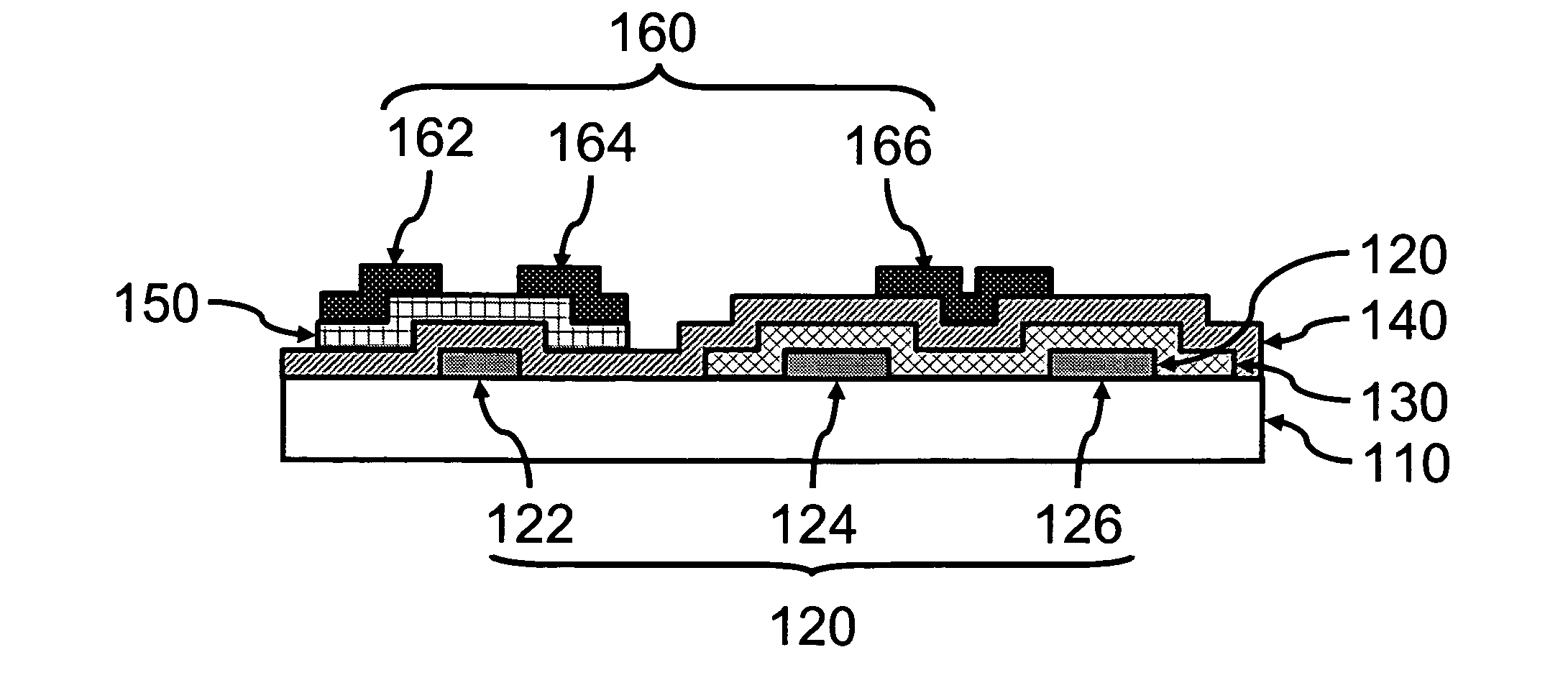
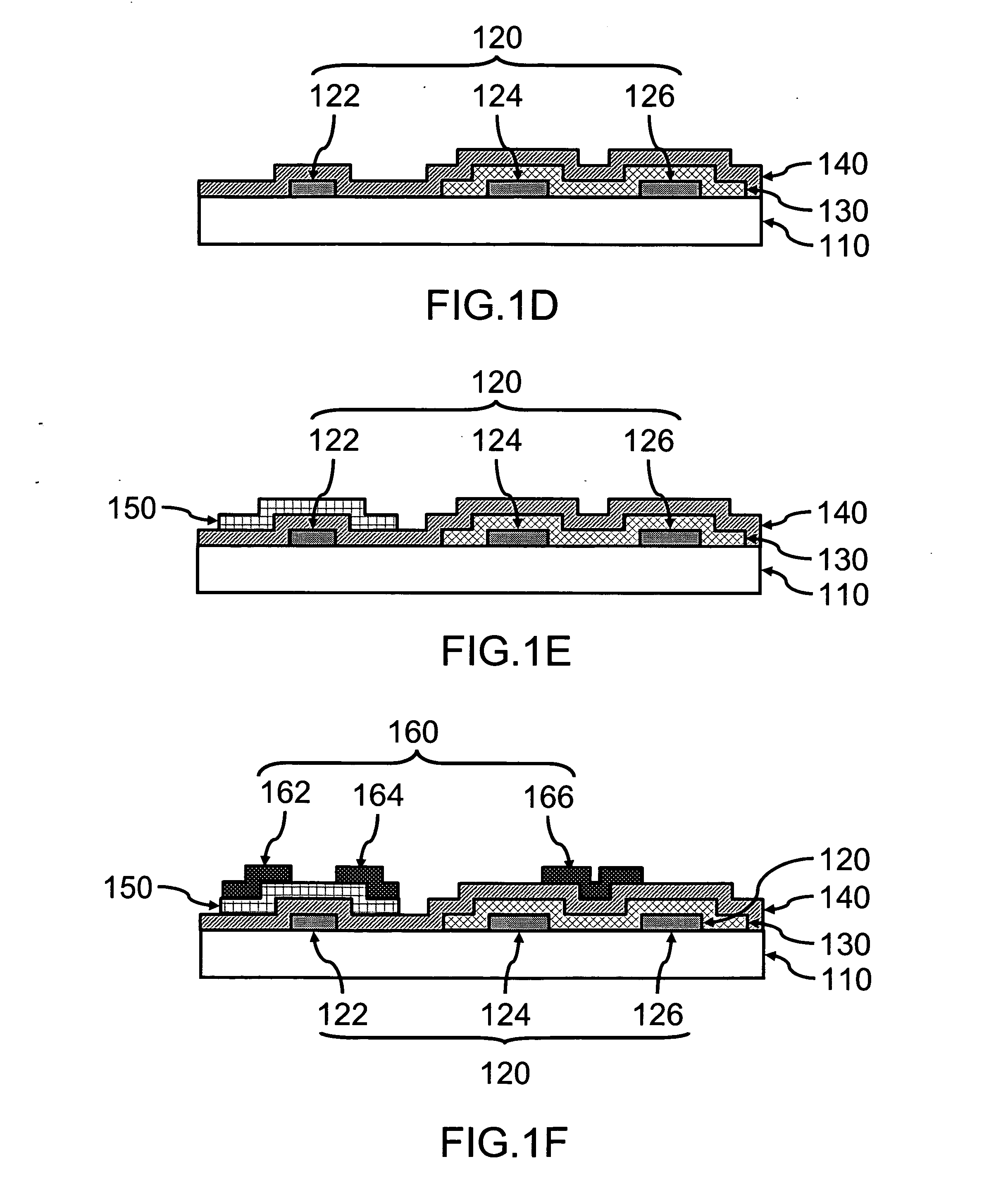
[0019] The concept of the invention is to make the electrodes to be electrically connected may connect with one another on the same layer, and directly connect the two terminals connected to one another by a conductive layer. This dramatically reduces the number of vias used based on practical circumstances.

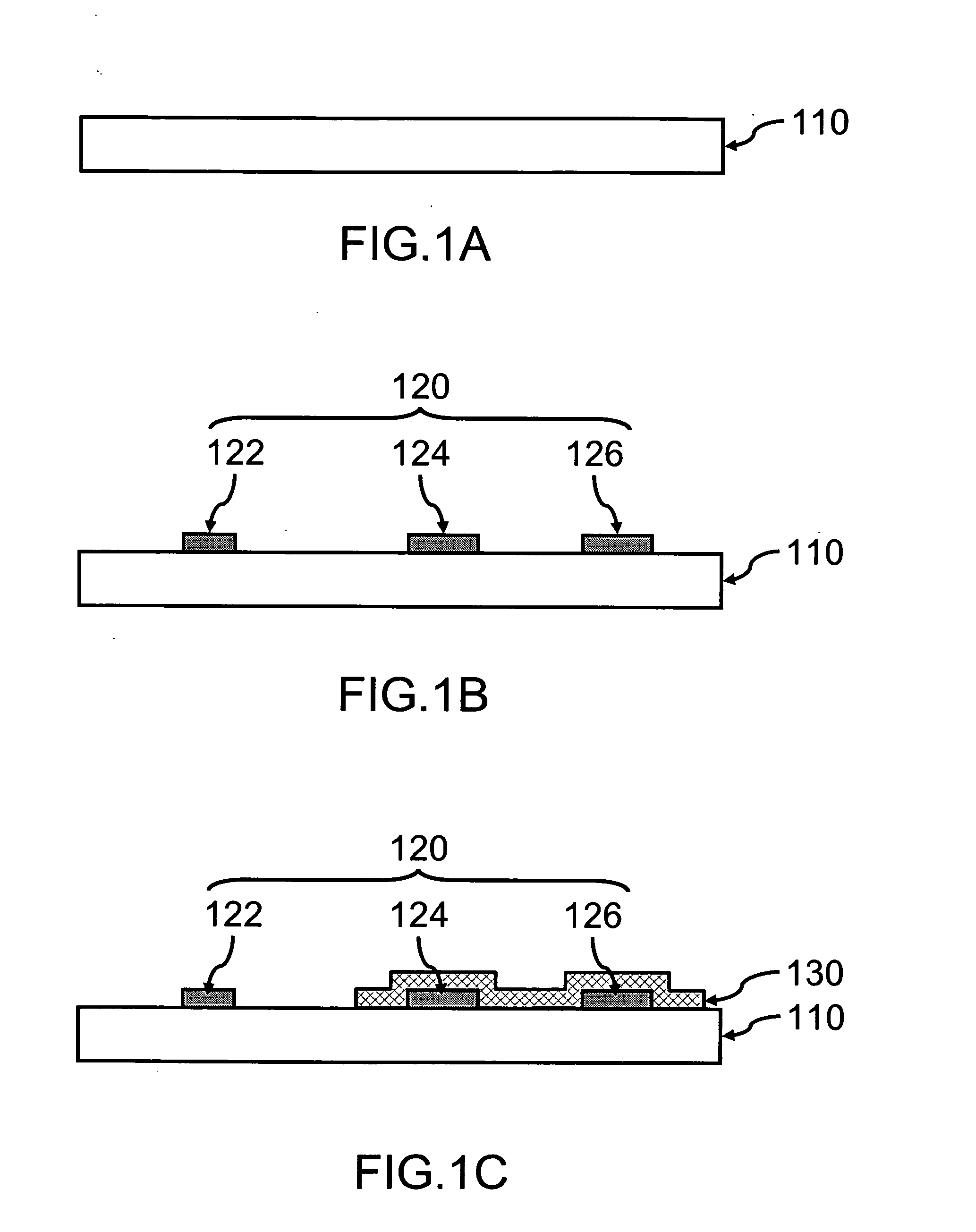
[0020] Please refer to FIGS. 1A to 1F, showing a flow chart of the fabricating method of the semiconductor device according to an embodiment of the invention. In FIG. 1A, a substrate 110 is provided.

[0021] The preferred material of the substrate is an isolating material, such as a polymer, a plastic or a glass. The material can be rigid or flexible and also can be a printing circuit board (PCB) material that includes an epoxy or a ceramic and has a silicon isolation layer or a silicon oxide isolation layer thereon.

[0022] Next, a first conductive layer 120 is formed on the substrate 110, where the first conductive layer 120 includes a first electrode region 122 (i.e. first elec...


PUM


Abstract

A semiconductor device with transistors and a fabricating method therefore are provided. The electrodes of the transistors are formed on the same layer, and they are coupled to one another by a conductor layer. Therefore, the requirement for the vias in whole circuit is reduced, and the cost is decreased.

Description

BACKGROUND [0001] 1. Field of Invention [0002] The invention relates to a semiconductor device and in particular to a semiconductor device with a plurality of transistors and a fabricating method therefor. [0003] 2. Related Art [0004] In a logic circuit, an inverter functions as a basic component. Therefore, whether a circuit is composed of a complementary metal oxide semiconductor (CMOS) inverter, an n-type metal oxide semiconductor (NMOS) inverter, a p-type metal oxide semiconductor (PMOS) inverter or a resistive load inverter, the circuit needs interconnections for the source-to-gate (namely a buffer or source / drain electrode output is used as the input of next circuit level), the source electrode to source / drain electrodes, or the gate to gate (ex. inverter component). Vias are utilized by the conventional method for establishing interconnections of circuits. [0005] A conventional process of establishing interconnection is described below. [0006] In the related art, a photolitho...

Claims


Application Information

Patent Timeline
Patent Type & Authority Applications(United States)
IPC IPC(8): H01L21/84H01L21/00H01L33/00H01L29/18
CPCH01L27/283H01L51/0541H01L51/0545H10K19/10H10K10/466H10K10/464
Inventor PEI, ZING-WAYKUNG, CHEN-PANG
Owner IND TECH RES INST
Why Eureka
Try Eureka