Method for manufacturing a semiconductor device having a stepped contact hole

a technology of contact hole and semiconductor, which is applied in the direction of semiconductor devices, electrical appliances, basic electric elements, etc., can solve the problems of difficult employing, difficult to perform stable etching therein, and the top portion of the contact hole may have an excessively large diameter or distorted sectional structure, etc., to achieve high etch selectivity of the dielectric and stable diameter

Inactive Publication Date: 2007-04-05
ELPIDA MEMORY INC
View PDF3 Cites 6 Cited by
  • Summary
  • Abstract
  • Description
  • Claims
  • Application Information

AI Technical Summary

Benefits of technology

[0016] In accordance with the method of the present invention, the first gas including the carbon-rich gas, which is richer than CF4 gas in the carbon content, allows the first anisotropic dry etching step to achieve a higher etch selectivity of the dielectric with respect to the photoresist mask compared to the etch selectivity in the anisotropic etching step of the conventional process using the CF4 gas. This provides a stable diameter for the first contact holes substantially without involving an etch stop failure in the first anisotropic dry etching step or a taper in the first contact hole.

Problems solved by technology

There is a problem in this anisotropic etching process, however, that the CF4-containing etching gas has a smaller etch selectivity between the mask pattern 33 and the dielectric film 32, whereby the top portion of the contact holes may have an excessively larger diameter or a distorted sectional structure.
This problem is especially crucial when a thin film photoresist mask is used for forming small-diameter contact holes, and thus is difficult to employ if a plurality of small-diameter contact holes are arranged at a higher density.
This process may involve an etch stop failure during the etching step due to the concurrent deposition step, and thus it is difficult to perform a stable etching therein.

Method used


Image

  • Method for manufacturing a semiconductor device having a stepped contact hole
  • Method for manufacturing a semiconductor device having a stepped contact hole
  • Method for manufacturing a semiconductor device having a stepped contact hole

Examples


Embodiment Construction

[0022] Now, the present invention is more specifically described with reference to accompanying drawings.

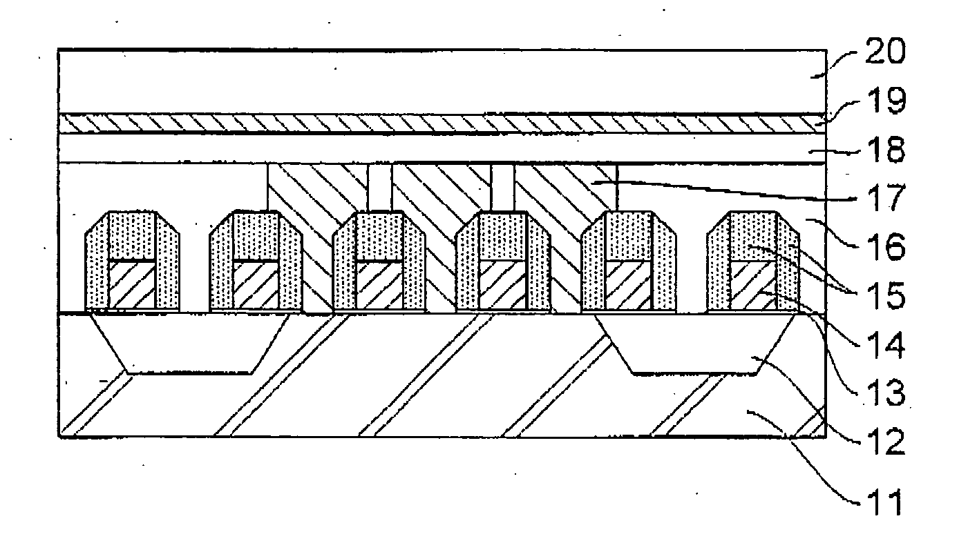
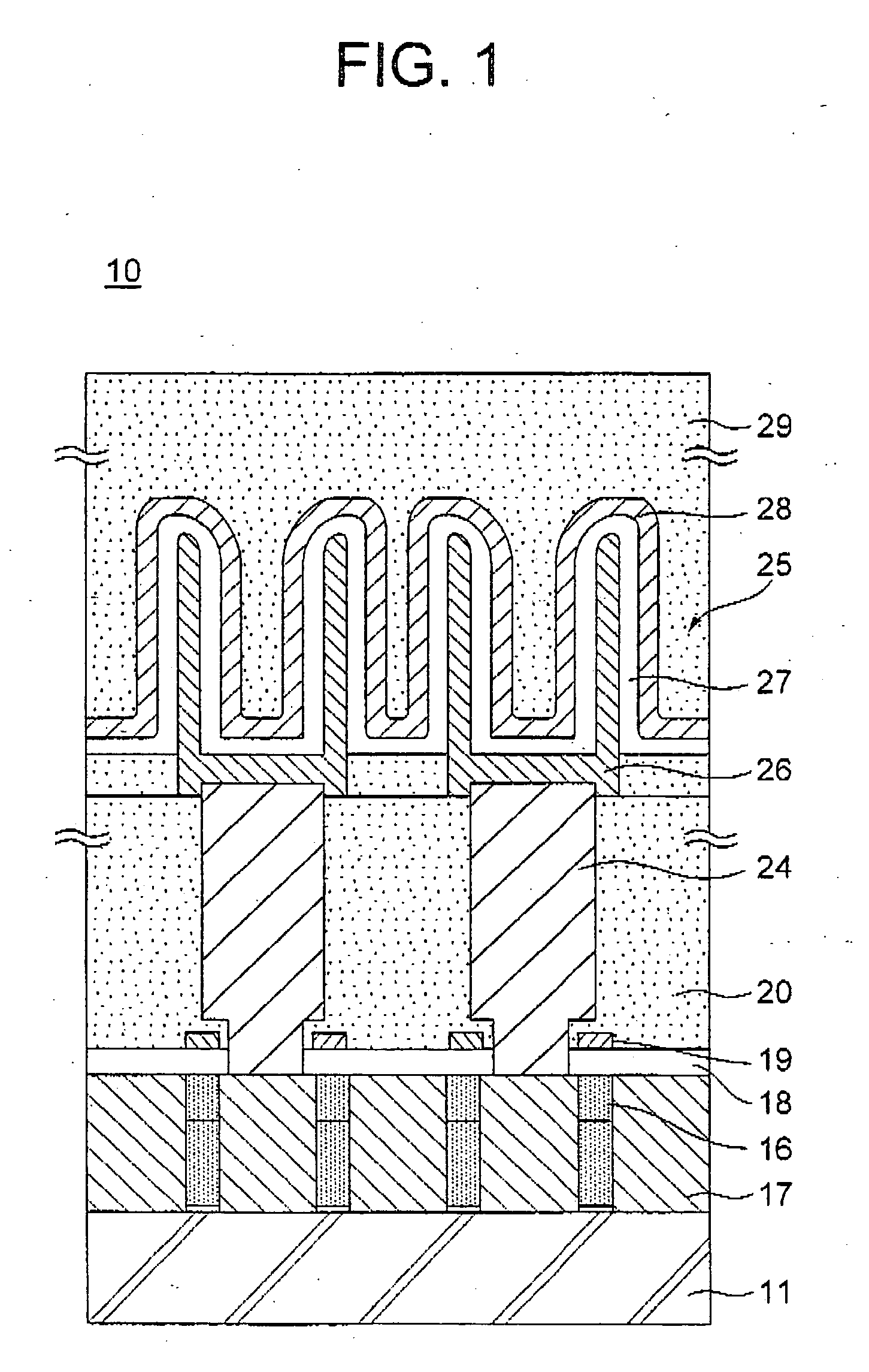
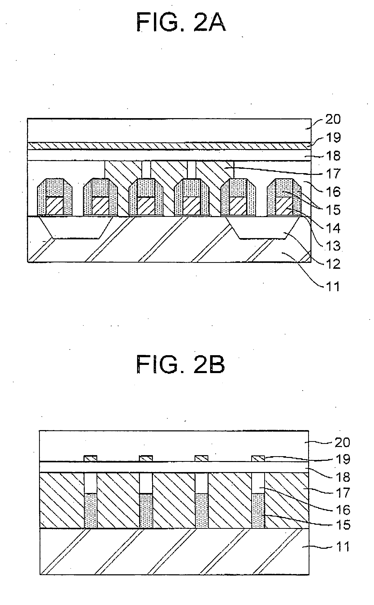
[0023]FIG. 1 shows a semiconductor device configured as a DRAM device, which is manufactured by a method according to an embodiment of the present invention. The DRAM device, generally designated by numeral 1Q, includes a semiconductor substrate 11 having diffused regions (not shown) on the surface region thereof. The diffused regions configure source / drain of cell transistors in contact with first contact plugs 17 penetrating through a first-layer dielectric film (silicon oxide film) 16. Second contact plugs 24 are in contact with top of the respective first contact plugs 17. The second contact plugs 24 penetrate through second- and third-layer dielectric films (silicon oxide films) 18, 20 and have a top in contact with bottom electrodes 26 of an overlying cell capacitors 25. The cell capacitors 25 include the bottom electrodes 26, capacitor insulation film 27 and top electrode...


PUM


Abstract

A process for forming a stepped contact hole includes: dry-etching a portion of a silicon oxide film using a mixed gas including carbon-rich fluorocarbon gas to form a first contact hole, forming a specific film on the sidewall of the first contact hole; dry-etching the remaining portion of the silicon oxide film at the bottom of the first contact hole by using the specific film as a mask to form a second contact hole extending from the first contact hole; and removing the specific film.

Description

BACKGROUND OF THE INVENTION [0001] (a) Field of the Invention [0002] The present invention relates to a method for manufacturing a semiconductor device having a stepped contact hole and, more particularly, to an improvement in forming a contact hole having a stepped structure including a top portion and a bottom portion having different diameters in a semiconductor device. [0003] (b) Description of the Related Art [0004] In a semiconductor device such as a DRAM device, an anisotropic etching process is generally used for forming a contact hole exposing the top of an underlying contact plug in contact with a diffused region of a semiconductor substrate. The contact hole to be formed by the anisotropic etching may be desired to have a stepped structure including a top portion having a large diameter and a bottom portion having a small diameter. The purpose for forming the small-diameter bottom portion is to allow the bottom portion to pass through a gap between adjacent interconnect l...

Claims


Application Information

Patent Timeline
Patent Type & Authority Applications(United States)
IPC IPC(8): H01L21/31
CPCH01L21/31116H01L21/31138H01L21/31144H01L21/76816H01L27/10855H01L2221/1057H10B12/0335
Inventor YOSHIDA, KAZUYOSHI
Owner ELPIDA MEMORY INC
Why Eureka
Try Eureka