Adaptive plasma source for generating uniform plasma

a plasma source and uniform technology, applied in the field of plasma semiconductor process, can solve the problems of uniform distribution of plasma generated inside the chamber, limit in solving these problems, etc., and achieve the effect of uniform plasma density

Inactive Publication Date: 2007-04-19
ADAPTIVE PLASMA TECH
View PDF5 Cites 363 Cited by
  • Summary
  • Abstract
  • Description
  • Claims
  • Application Information

AI Technical Summary

Benefits of technology

[0028] According to the adaptive plasma source of the present invention, unit coils are arranged around a bushing in a spiral shape based on a predetermined rule so that the coil arrangement can be symmetrical in any position. Thus, a uniform plasma density can be achieved. Also, due to the bushing disposed at a central portion, plasma densi

Problems solved by technology

Like this, if the amount of current becomes ununiform, a distribution of plasma generated inside the chamber also becomes un

Method used


Image

  • Adaptive plasma source for generating uniform plasma
  • Adaptive plasma source for generating uniform plasma
  • Adaptive plasma source for generating uniform plasma

Examples


Embodiment Construction

Technical Goal of the Invention

[0017] The present invention provides an adaptive plasma source that forms uniform plasma inside a plasma reaction chamber.

Disclosure of the Invention

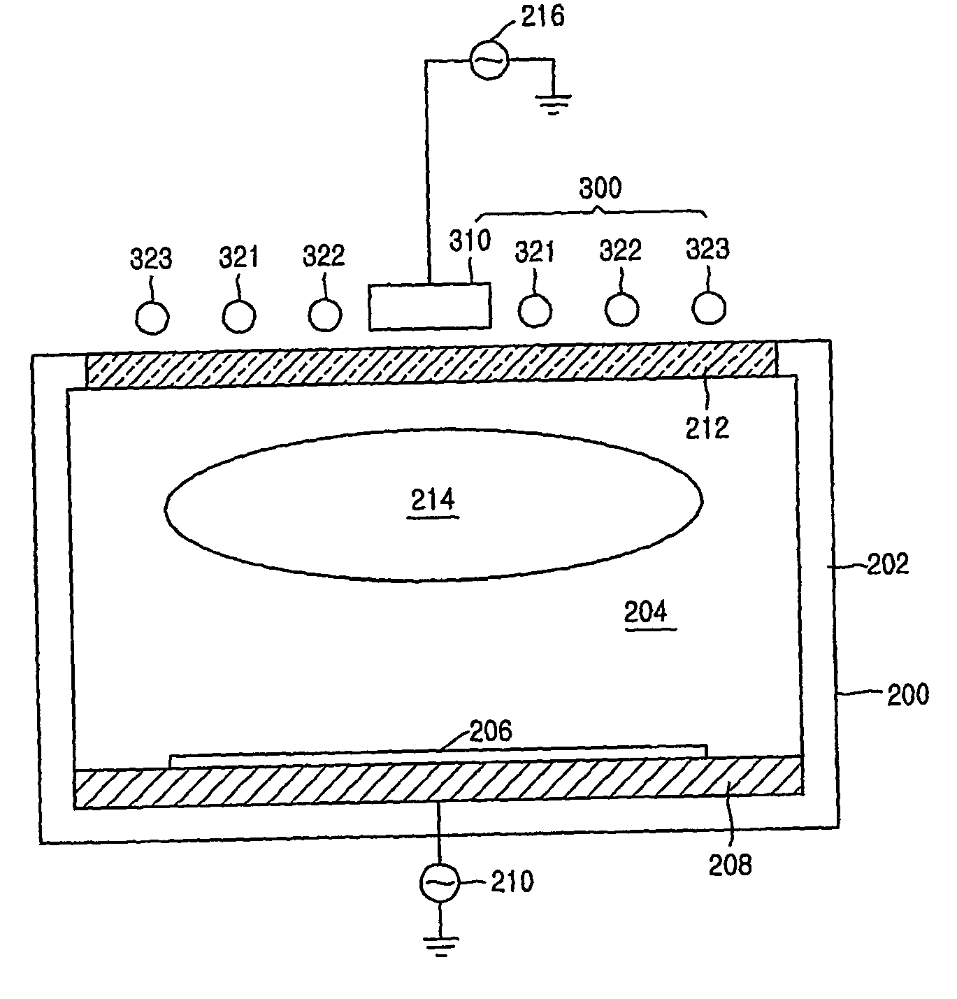
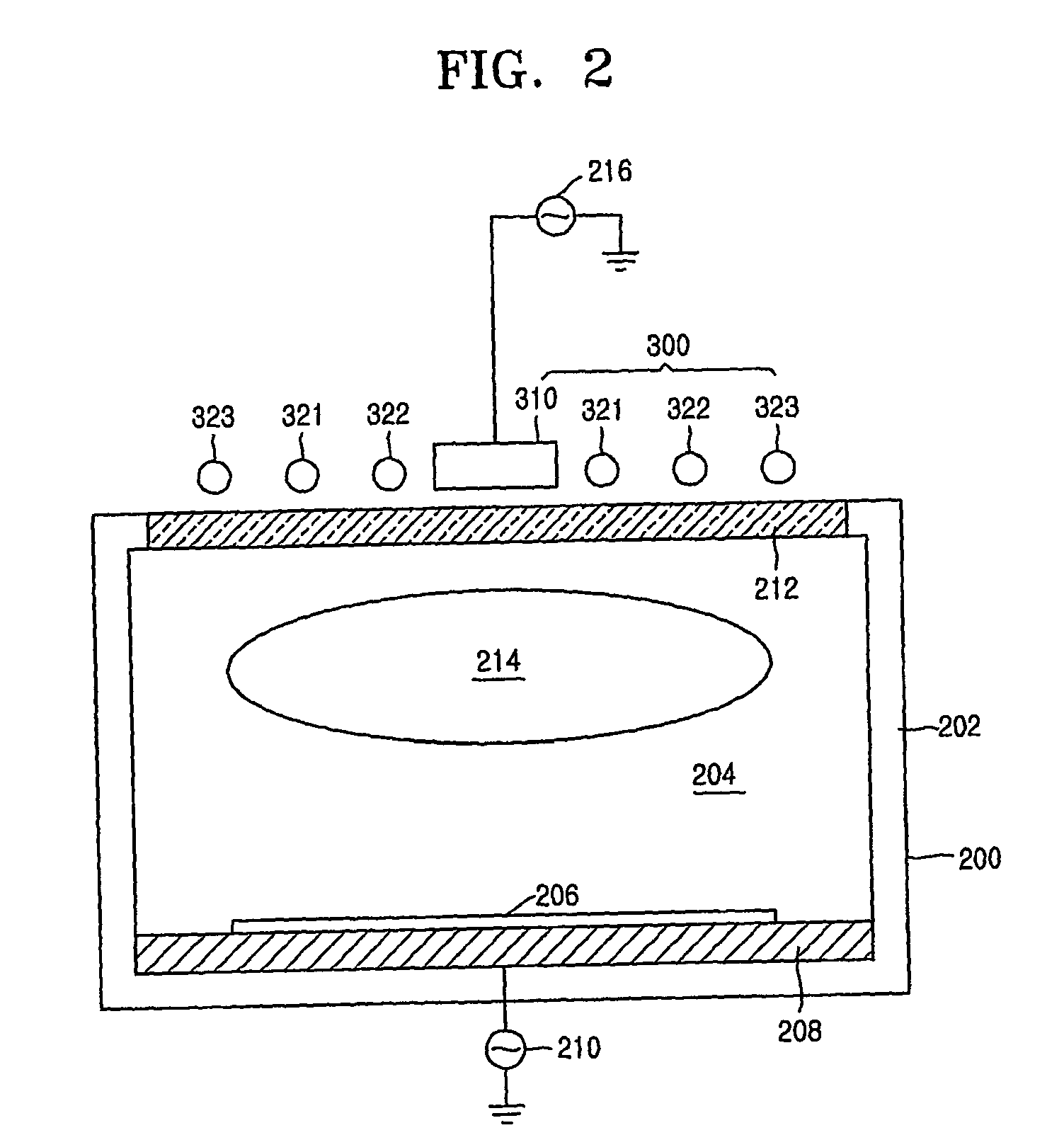
[0018] According to an aspect of the present invention, there is provided an adaptive plasma source arranged at an upper portion of a reaction chamber having a reaction space to form plasma and supplied with RF (radio frequency) power from an external RF power source to form an electric field inside the reaction space. The adaptive plasma source includes: a conductive bushing coupled to the RF power source and arranged at an upper central portion of the reaction chamber; and at least two unit coils branched from the bushing, the unit coils surrounding the bushing in a spiral shape and having a number of turns equal to a×(b / m), where a and b are positive integers and m is the number of the unit coils.

[0019] The bushing may have a circular shape with a predetermined diameter and the unit coils may be br...


PUM

PropertyMeasurementUnit
Timeaaaaaaaaaa
Diameteraaaaaaaaaa
Shapeaaaaaaaaaa

Abstract

There is provided an adaptive plasma source, which is arranged at an upper portion of a reaction chamber having a reaction space to form plasma and is supplied with RF (radio frequency) power from an external RF power source to form an electric field inside the reaction space. The adaptive plasma source includes a conductive bushing and at least two unit coils. The bushing is coupled to the RF power source and arranged at an upper central portion of the reaction chamber. The at least two unit coils are branched from the bushing and surround the bushing in a spiral shape and have the number of turns equal to a×(b/m), where a and b are positive integers and m is the number of the unit coils.

Description

TECHNICAL FIELD [0001] The present invention relates to plasma semiconductor process, and more particularly, to an adaptive plasma source for generating uniform plasma inside a plasma reaction chamber. BACKGROUND ART [0002] Technologies for fabricating ultra-large scale integration (ULSI) circuit devices have remarkably developed during the last 20 years. Owing to semiconductor fabrication pieces of equipment using cut-edge technologies. A plasma reaction chamber, one of the semiconductor fabrication pieces of equipment, is used in a deposition process as well as an etching process and its application has widely increased. [0003] Plasma is formed inside the plasma reaction chamber and used in an etching process, a deposition process, and the like. Based on plasma sources, plasma reaction chambers are classified into various types: an electron cyclotron resonance (ECR) plasma source, a helicon-wave-excited plasma (HWEP) source, a capacitively coupled plasma (CCP) source, and an induc...

Claims


Application Information

Patent Timeline
IPC IPC(8): C23F1/00C23C16/00H01J37/32H05H1/46
CPCH01J37/321H05H1/46
Inventor KIM, NAM-HUN
Owner ADAPTIVE PLASMA TECH
Why Eureka
Try Eureka