Electron beam applying apparatus and drawing apparatus

a technology of electromagnetic beam and applying apparatus, which is applied in the field of electromagnetic beam applying apparatus and drawing apparatus, can solve the problems of inability to carry out data writing by optical mastering apparatus, inability to sufficiently reduce the beam diameter, and difficulty in sufficiently condensing, so as to reduce the hole diameter of the hole part, reduce the beam diameter, and the effect of low cos

Inactive Publication Date: 2007-04-19
RICOH KK +1
View PDF5 Cites 11 Cited by
  • Summary
  • Abstract
  • Description
  • Claims
  • Application Information

AI Technical Summary

Benefits of technology

[0038] Furthermore, since the electron beam applying apparatus according to the present invention has a very simple configuration in which the thermal field emission type electron source is applied, and the electrostatic lens is disposed, it is possible to generate an electron beam with a large electric current with a minimal beam diameter at a low cost.
[0039] Further, by setting the crossover point in the proximity to the hole part of the aperture acting both as the selector aperture and as the objective aperture, it is possible to reduce the hole diameter of the hole part, and to reduce a deflection amount of the electron beam for blanking. Thereby, it is possible to make the blanking voltage relatively low, and to increase an electron beam tuning on / off switching frequency for blanking. That is, it is possible to achieve high speed drawing.
[0040] Further, in the electron beam applying apparatus according to the present invention, the axis aligning coil and the blanking electrode are disposed apart. Accordingly, even when a large electric current is made to flow through the blanking electrodes for the purpose of increasing the electron beam turning on / off switching frequency for blanking, its electromagnetic interference does not occur in the axis aligning coil. As a result, it is possible to avoid a situation in which magnetic field occurs in the axis aligning coils, the electron beam is bent, and thus, an axis error occurs in the electron beam.
[0041] Further, in the drawing apparatus according to the present invention, since information is recorded on a surface of a material with the use of an electron beam emitted by any one of the above-mentioned electron beam applying apparatuses, it is possible to carry out, with a simple configuration at a low cost, drawing at high speed with the use of the electron beam with a large electric current and a minimal beam diameter.

Problems solved by technology

However, since a pit pattern of a next-generation Blu-ray Disk or a pattern dimension of a further-next-generation DVD is very small, data writing cannot be carried out by an optical mastering apparatus.
Accordingly, it becomes difficult to sufficiently condense the electron beam by means of the objective lens 66, and thus, it may not be possible to sufficiently reduce the beam diameter, or the beam diameter of the electron beam increases.
However, since the beam diameter reduction ratio of the electron beam is thus made smaller, this method can be applied only for a case where the beam diameter of the electron beam emitted by the electron source 52 is originally small, and this method cannot be applied for a case where the beam diameter is originally large, and thus, the beam diameter should be reduced.
Further, as the two apertures are thus applied, a mechanical error may occur therebetween, and the hole parts thereof may not be aligned on the same axis accurately.
As a result, a relatively high voltage is required as a blanking voltage, and thus, an increase of a turning on / off switching frequency of the electron beam for blanking becomes difficult.
That it, an increase in the drawing speed may not be possible.
Thereby, an axis shift of the electron beam in the axis aligning coils 56 may cause a large problem in this case.

Method used


Image

  • Electron beam applying apparatus and drawing apparatus
  • Electron beam applying apparatus and drawing apparatus
  • Electron beam applying apparatus and drawing apparatus

Examples


Embodiment Construction

[0048] Based on a preferable embodiment shown in figures, an electron beam applying apparatus and a drawing apparatus employing it according to the present invention are described in detail.

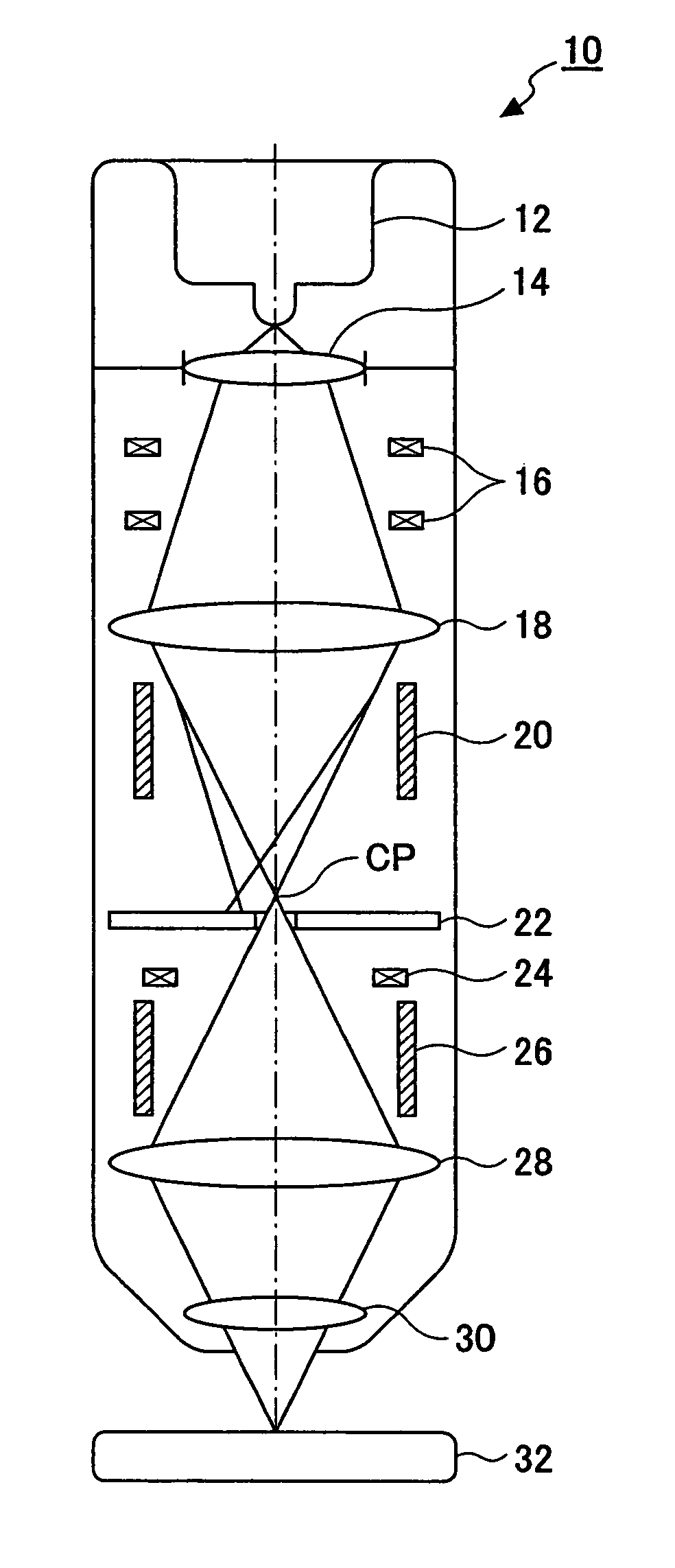
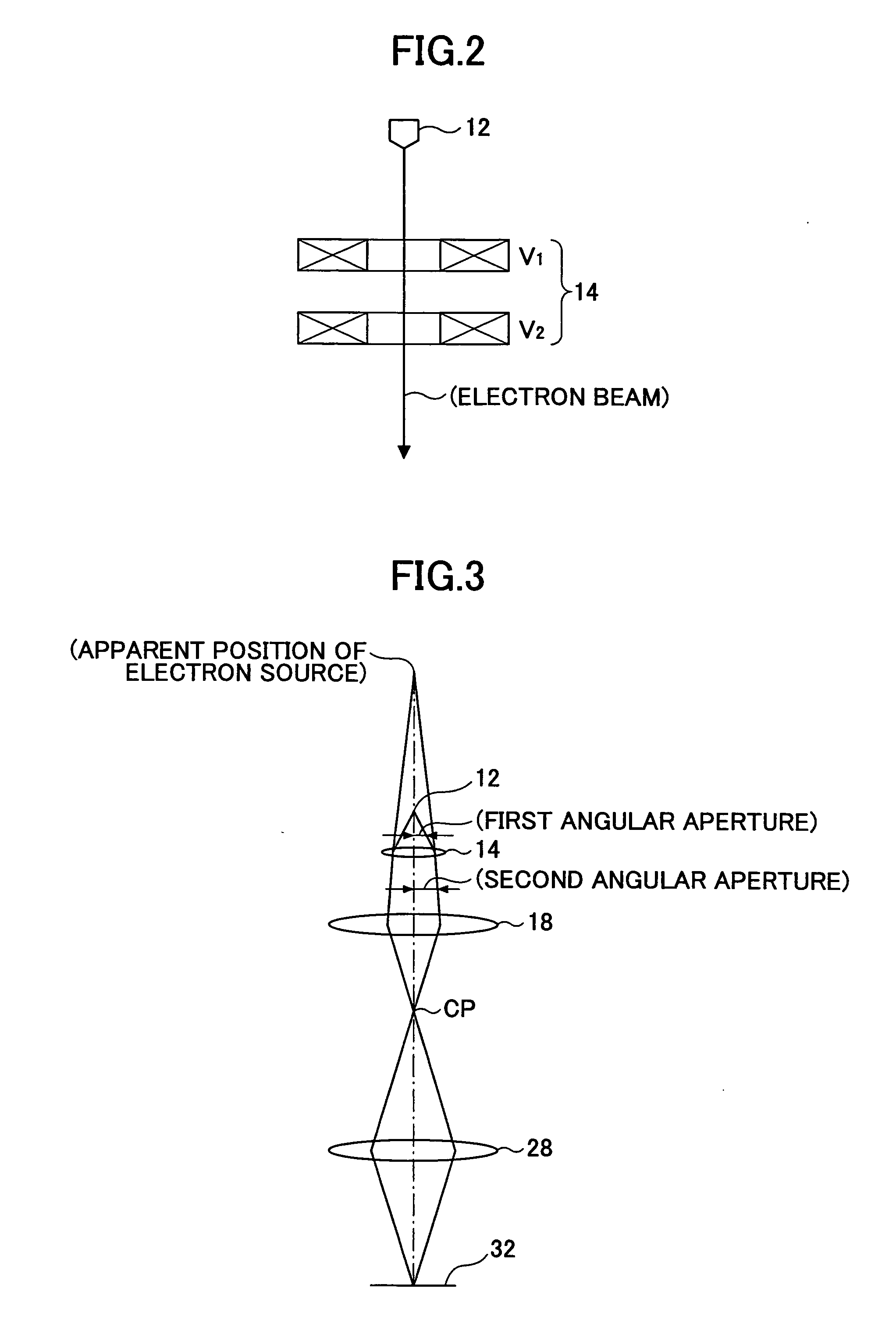
[0049]FIG. 1 shows an outline of an embodiment of an electron beam applying apparatus according to the present invention. The electron beam applying apparatus 10 shown is used to apply an electron beam on a surface of a material 32 for the purpose of recording information on the surface of the material 32 (for example, an optical medium such as a DVD), and includes an electron source 12, an electrostatic lens 14, axis aligning coils 16, a condenser lens 18, blanking electrodes 20, an aperture 22 acting both as a selector aperture and as an objective aperture, an astigmatism correction coil 24, electrostatic deflection electrodes 26, an objective lens 28 and a dynamic focal correction lens 30.

[0050] In the electron beam applying apparatus 10 shown, the electron source (electron gun) 12 is of a t...


PUM


Abstract

An electron beam applying apparatus includes: a thermal field emission type electron source emitting an electron beam; an electrostatic lens disposed immediately below the electron source and acting as a condensing electrode for condensing the electron beam in a first angular aperture emitted by the electron source in a second angular aperture smaller than the first angular aperture; a condenser lens disposed on a downstream side of the electrostatic lens and condensing the electron beam condensed in the second aperture angel by the electrostatic lens in a crossover point; and an objective lens disposed on a downstream side of the condenser lens and condensing the electron beam condensed in the crossover point by the condenser lens on the surface of the material.

Description

TECHNICAL FIELD [0001] The present invention relates to an electron beam applying apparatus applying an electron beam on a surface of a material for recording information on the surface of the material, and a drawing apparatus recording information on a surface of a material with the use of an electron beam applied by the electron beam applying apparatus. BACKGROUND ART [0002] Currently, a DVD (digital versatile disk), which is an optical recording medium having a large storage capacity for which data writing or re-wiring is allowed, exists. A storage capacity of a current DVD-R (recordable) or a DVD-RW (re-writeable) is 4.7 GB (gigabytes) for one side in a single layer, and it has a pattern dimension in which a groove width is on the order of 400 nm, and a track pitch (a width between grooves) is on the order of 740 nm. [0003] In contrast thereto, as a next-generation DVD, an HD-DVD (high definition DVD) exists. A storage. capacity of HD-DVD is on the order of 15 GB for one side in...

Claims


Application Information

Patent Timeline
Patent Type & Authority Applications(United States)
IPC IPC(8): G21K7/00
CPCG11B7/0045G11B7/261G11B9/10G11B11/002H01J37/3007H01J2237/3175
Inventor MIYAZAKI, TAKESHIOHYI, HIDEYUKIOBARA, TAKASHI
Owner RICOH KK
Why Eureka
Try Eureka