Semiconductor device and fabrication method thereof
Inactive Publication Date: 2007-04-19
LAPIS SEMICON CO LTD
View PDF9 Cites 16 Cited by
Summary
Abstract
Description
Claims
Application Information
AI Technical Summary
This helps you quickly interpret patents by identifying the three key elements:
Problems solved by technology
Method used
Benefits of technology
Benefits of technology
[0012] It is one object of the present invention to provide a semiconductor device having a W-CSP structure which can increase pins while improving the bonding strength of the columnar electrodes and solder balls, without increasing the diameter of the solder ball (or the diameter of the external terminal.
[0013] Another object of the present invention is to provide a simple fabrication method for such semiconductor device.
[0015] According to this semiconductor device, the column-shaped electrode itself is cut from the top face, and the protrusion section and trench (or recess) are formed in the column-shaped electrode. At the same time, part of the sealing section is also removed so that side faces of the protrusion section are exposed. Thus, the top face and side faces of the protrusion section can be used as a bonding face. Accordingly, the shape of the bonding face between the electrode and solder ball becomes more complicated and the bonding area is increased. Therefore, the bonding strength between the electrode and solder ball can be dramatically improved. Also the diameter of the solder ball is not increased by this, so that a further increase in pins can be implemented.
[0016] It should be noted that instead of the trench sections, there may be formed a recess in the top of the protrusion of each electrode. At least part of the solder ball is received in the recess when the solder ball is attached to the electrode. The recess increases the bonding area between the electrode and solder ball so that the bonding strength between the electrode and solder ball is increased.
[0019] According to this fabrication method of the semiconductor device, the trench section can be formed by a simple cutting process using a blade, such as a dicing saw of a dicing device, for example, so that a semiconductor device having the above described advantages can be fabricated efficiently.
Problems solved by technology
Accordingly, the shape of the bonding face between the electrode and solder ball becomes more complicated and the bonding area is increased.
Method used
Image
Click on the blue label to locate the original text in one second.
Reading with bidirectional positioning of images and text.
Examples
first embodiment
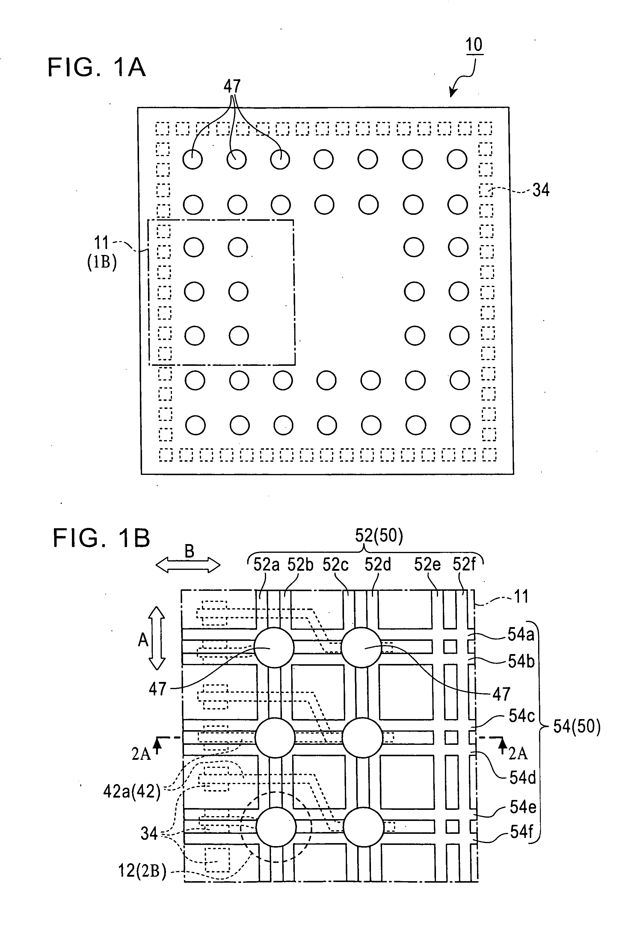
[0036] The configuration of the semiconductor device 10 according to the first embodiment will now be described with reference to FIGS. 1A, 1B, 2A and 2B.
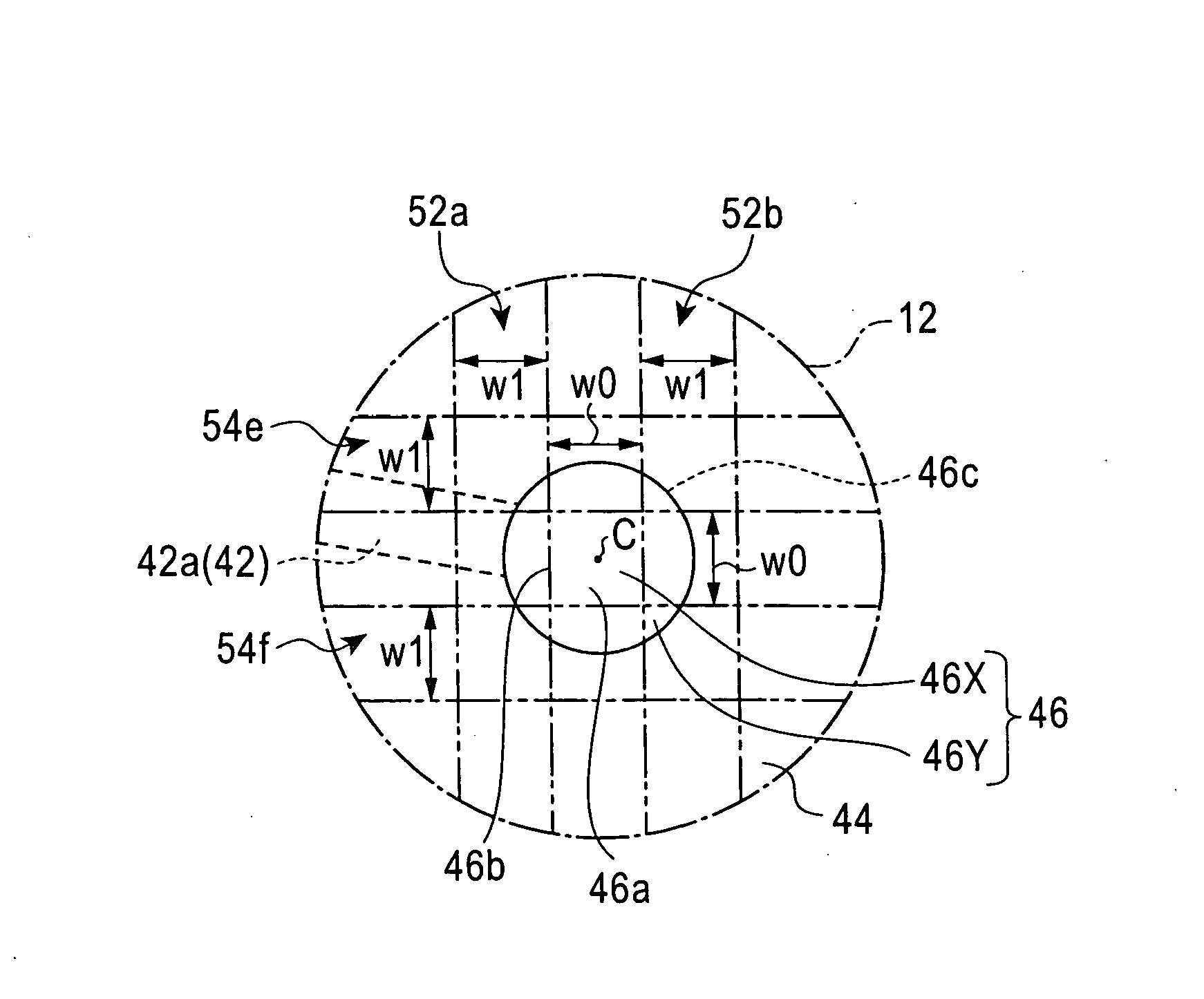
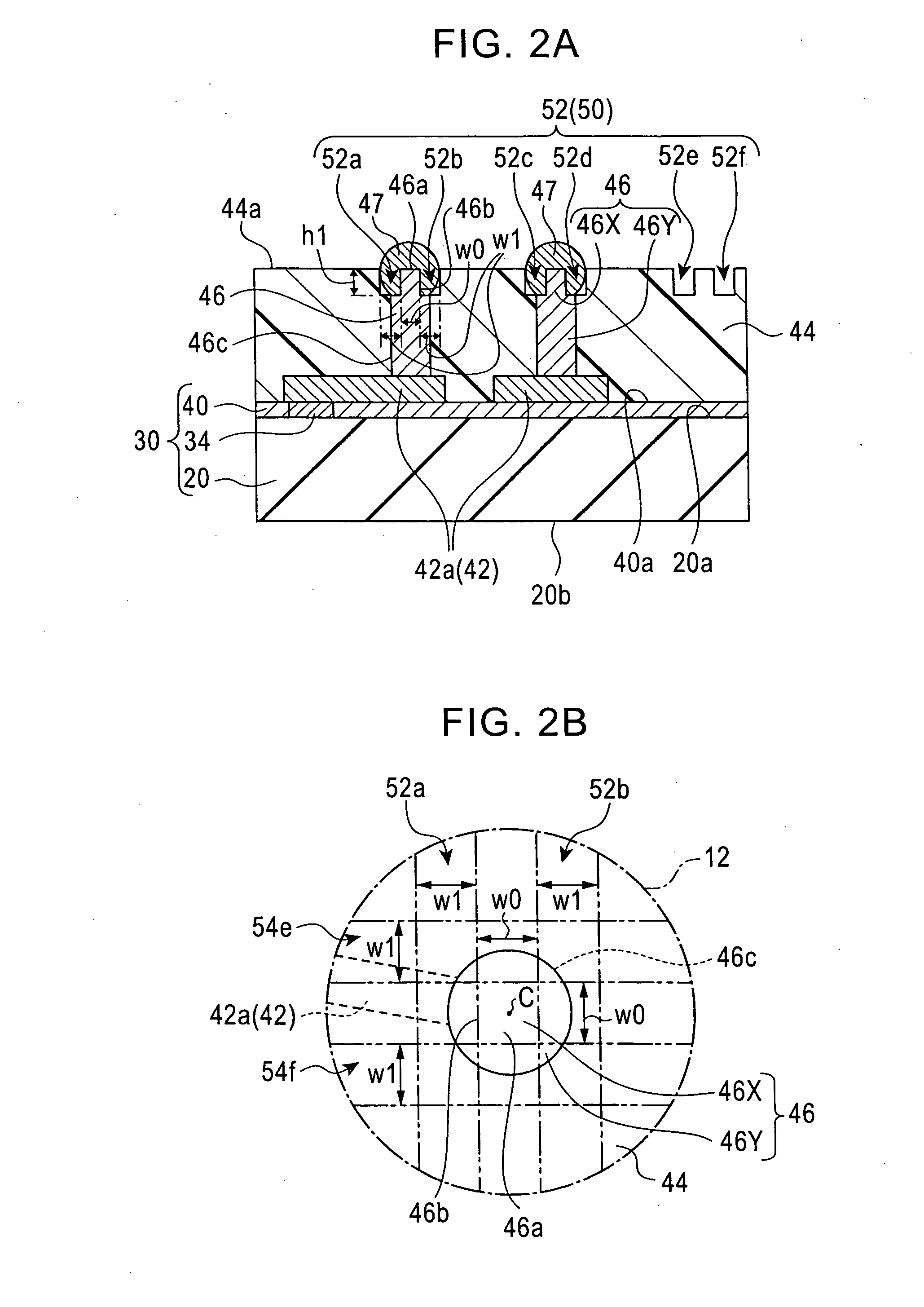
[0037]FIG. 1B is an enlarged plan view depicting the detail of the first partial area 11 enclosed by the solid line in FIG. 1A. FIG. 2B is an enlarged plan view depicting the detail of the second partial area 12 indicated by the dotted line in FIG. 1B. In FIG. 2B, the solder ball 47, which actually exists, is omitted to describe the structure below the solder ball.
[0038] In particular as shown in FIG. 2A, the semiconductor device (W-CSP) 10 includes a semiconductor chip 30 on the silicon (Si) substrate. The semiconductor chip 30 has circuit elements and various functional elements. The circuit element (not illustrated) formed in the thickness of the semiconductor chip 30 includes a plurality of active elements having integrated circuits, such as LSI, so as to implement a predetermined function. In the circuit element, a multilaye...
second embodiment
[0096] Now the second embodiment of the present invention will be described with reference to FIGS. 5A, 5B, 5C, 6A and 6B.
[0097] The same composing elements as the first embodiment are denoted with the same reference symbols, and detailed description thereof will be omitted. However, among such composing elements, those required for understanding the configuration of the semiconductor device of the second embodiment will be described in brief.
[0098] A configuration of the semiconductor device of the present embodiment will be described first with reference to FIGS. 5A, 5B and 5C. The plan view of the semiconductor device 10 of this embodiment is omitted since it is exactly the same as FIG. 1A.
[0099]FIG. 5A is similar to FIG. 1B. FIG. 5A is an enlarged plan view of major portions of the semiconductor device 10, depicting the area corresponding to the first area 11 enclosed by the solid line 11 in FIG. 1A. FIG. 5B is a cross-sectional view taken along the dashed line 5B-5B in FIG. ...
third embodiment
[0133] The third embodiment of the present invention will now be described with reference to FIGS. 7A, 7B, 7C, 8A and 8B.
[0134] The same composing elements as the first embodiment are denoted with the same reference symbols, and detailed description thereof will be omitted. However, among such composing elements, those required for understanding the configuration of the third embodiment will be described briefly.
[0135] The semiconductor device of the third embodiment will now be described with reference to FIGS. 7A to 7C. The plan view of the semiconductor device 10 of this embodiment is exactly the same as FIG. 1A, so that an illustration is omitted.
[0136]FIG. 7A is similar to FIG. 1B. Specifically, FIG. 7A is an enlarged plan view of major portions of the semiconductor device 10 depicting an area corresponding to the first partial area 11 enclosed by the solid line in FIG. 1A. FIG. 7B is a cross-sectional view taken along the dashed line 7B-7B in FIG. 7A. FIG. 7C is an enlarged...
PUM
Abstract
A semiconductor device includes a semiconductorchip having a plurality of electrode pads, and a rewiring pattern having a plurality of interconnects which are connected to the electrode pads and extend over an insulation film. The semiconductor device also includes a plurality of columnar electrodes each of which has a main body section and a protrusion section, and a sealing section which has a top face having a height the same as the top faces of the protrusion sections. The semiconductor device also includes solder balls formed on the protrusion sections. The semiconductor device also has a plurality of trenches in the sealing section. Each trench has a depth which reaches the boundary between the main body and protrusion of the electrode. The side faces of the protrusion section are exposed face defined by the trenches. Each solder ball is electrically connected to the top face and side faces of the protrusion section of each electrode.
Description
BACKGROUND OF THE INVENTION [0001] 1. Field of the Invention [0002] The present invention relates to a semiconductor device having a so-called W-CSP (Wafer Level Chip Size Package) and a fabrication method thereof. [0003] 2. Description of the Related Art [0004] A semiconductor chippackage, of which size is almost equal to that of a semiconductor chip diced from a semiconductor wafer, is generally called a CSP (Chip Size Package). A CSP created by packaging a semiconductor chip having predetermined functions formed in a semiconductor wafer, in semiconductor wafer status, and then dicing it into an individual chip, in particular is called a W-CSP. [0005] In such CSPs, an external terminal is a columnar electrode (post-like electrode) or a combination of a columnar electrode and a solder ball. The solder ball is connected to the top face of the columnar electrode. [0006] If the electrode terminal is a columnar electrode having a solder ball thereon, an alloy portion is inevitably for...
Claims
Application Information
Patent Timeline
Application Date:The date an application was filed.
Publication Date:The date a patent or application was officially published.
First Publication Date:The earliest publication date of a patent with the same application number.
Issue Date:Publication date of the patent grant document.
PCT Entry Date:The Entry date of PCT National Phase.
Estimated Expiry Date:The statutory expiry date of a patent right according to the Patent Law, and it is the longest term of protection that the patent right can achieve without the termination of the patent right due to other reasons(Term extension factor has been taken into account ).
Invalid Date:Actual expiry date is based on effective date or publication date of legal transaction data of invalid patent.

