
Semiconductor optical device having a clamped carrier density

Inactive Publication Date: 2007-04-19
ALCATEL LUCENT SAS
View PDF11 Cites 0 Cited by
  • Summary
  • Abstract
  • Description
  • Claims
  • Application Information

AI Technical Summary

Problems solved by technology

All these drawbacks are essentially due to the fact that the laser power remains dependent on the intensity of the current injected into the active zone.

Method used


Image

  • Semiconductor optical device having a clamped carrier density
  • Semiconductor optical device having a clamped carrier density
  • Semiconductor optical device having a clamped carrier density

Examples


Embodiment Construction

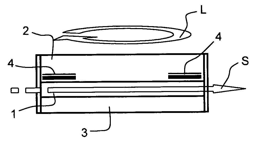
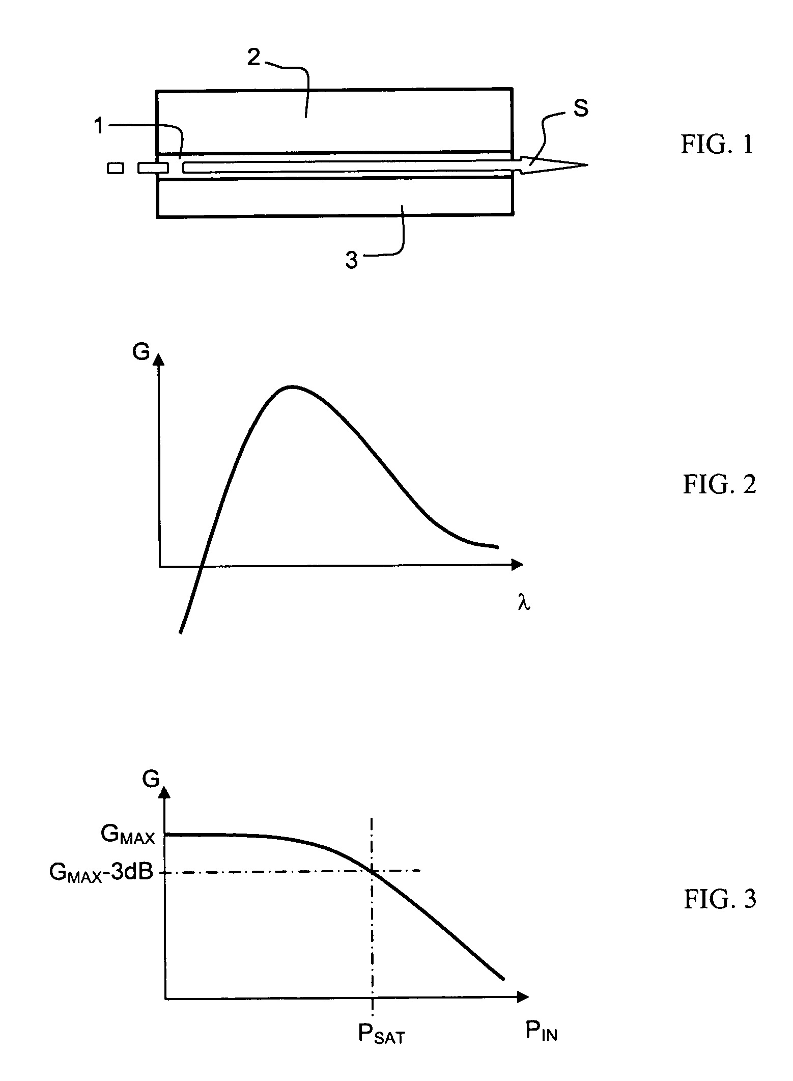
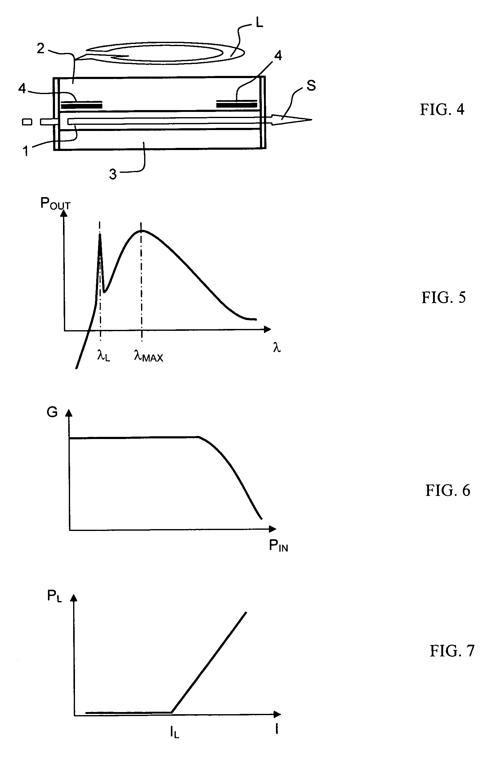
[0034] The quantum dots are microstructures that contain a small quantity of charge carriers, free electrons or holes. They are fabricated in semiconductor-type materials and have dimensions between a few nanometres and a few tens of nanometres in the three dimensions of space. The size and shape of these structures, and therefore the number of holes that they contain, may thus be precisely controlled. As in an atom, the energy levels in a quantum dot are quantized, which makes these structures particularly advantageous for a large number of physical applications.

[0035] As shown in FIG. 8, only two possible energy transition states may exist in a quantum dot structure, called the ground state (GS) and the excited state (ES), the ground state corresponding to the lowest energy level. These two transition states correspond to the two vertical arrows shown in FIG. 8. Corresponding to these two transition states are two emission wavelengths, denoted by λES and λGS. As already mentioned...


PUM


Abstract

The field of the invention is that of semiconductor devices used for the amplification or for the phase modulation of optical signals. These devices are known by the generic names SOA (semiconductor optical amplifier) and DPSK (differential phase shift keying) modulators. The main drawbacks of this type of device are that it is, on the one hand, difficult to obtain a constant gain, and, on the other hand, it is difficult for the optical signal to be independently amplitude-modulated and phase-modulated. The device according to the invention does not have these drawbacks. It relies essentially on three principles: the active zone of the device has a quantum dot structure, the atoms of said structure possessing a first energy transition state called the ground state and a second energy transition state called the excited state; the active zone is placed in a structured resonant cavity in order to resonate at a first wavelength corresponding to the ground state; and the current flowing through the active zone is greater than the saturation current of the ground state so as to allow oscillation at a second wavelength corresponding to the excited state.

Description

RELATED APPLICATION [0001] The present application is based on, and claims priority from France Application Number 05 10512, filed Oct. 14, 2005, the disclosure of which is hereby incorporated by reference herein in its entirety. BACKGROUND OF THE INVENTION [0002] 1. Field of the Invention [0003] The field of the invention is that of semiconductor devices used for the amplification or for the phase modulation of optical signals. The devices used for amplification are known by the generic name SOA (semiconductor optical amplifier). [0004] 2. Description of the Prior Art [0005] Current semiconductor devices used for the amplification or the modulation of optical signals have several drawbacks. [0006] Firstly, the variations in optical gain of the active medium are intrinsically linked to the variations in its optical index, the gain variations resulting in amplitude variations of the optical signals, and the optical index variations resulting in phase variations. Under these condition...

Claims


Application Information

Patent Timeline
IPC IPC(8): H01S3/00H01S5/12
CPCB82Y20/00H01S5/12H01S5/341H01S5/50H01S5/5072
Inventor DAGENS, BEATRICE
Owner ALCATEL LUCENT SAS
Features
  • Generate Ideas
  • Intellectual Property
  • Life Sciences
  • Materials
  • Tech Scout
  • Unparalleled Data Quality
  • Higher Quality Content
  • 60% Fewer Hallucinations
Learn More