Semiconductor device and method of manufacture thereof

a semiconductor device and semiconductor technology, applied in the direction of semiconductor devices, semiconductor/solid-state device details, electrical apparatus, etc., can solve the problems of difficult to fill the trenches for the formation of sealing layers with resin materials, and the semiconductor device is not suitable for use,

Inactive Publication Date: 2007-04-26
RENESAS ELECTRONICS CORP
View PDF5 Cites 92 Cited by
  • Summary
  • Abstract
  • Description
  • Claims
  • Application Information

AI Technical Summary

Benefits of technology

[0046] As described above, the seal ring is formed of a layered body of conductive sealing layers which are respectively provided in a plurality of interlayer insulating films that form multilevel wiring layers, and the layered body of the sealing layers has a portion where a plurality of first sealing layers of which the cross sectional form is in T-shape are layered in sequence and a portion where a plurality of second sealing layers of which the cross sectional form is rectangular are layered in sequence, and thus, a plurality of first sealing layers are layered in sequence on the lower layer side of the multilevel wiring layers and a plurality of second sealing layers are layered in sequence on the upper layer side in the configuration, and thereby, the structure of the seal ring is optimized, the physical strength is increased and a function as a barrier against the penetration of moisture from the cut section along the dicing portion and the spreading of cracks can be secured.

Problems solved by technology

These interlayer insulating films and interfaces between the interlayer insulating films become paths for moisture to penetrate, and there is a possibility that these may become a problem in terms of reliability in such a manner that these may cause a malfunction of the semiconductor device.
In addition, cracking may occur in the interlayer insulating films due to stress at the time of dicing or stress caused by a difference in the coefficient of thermal expansion between the interlayer insulating films and the molding resin that is used at the time of the packaging of the LSI chip, and this cracking may become a path for moisture to penetrate.
In particular, the volume of the sealing layers, which are formed in the same process for the contact portions, is extremely large in comparison with the contact portions, and therefore, it is technically difficult to fill the trenches for the formation of these sealing layers with a resin material.
In the case where etching is carried out in order to create trenches, which become wiring layers in a state where filling with the resin material is insufficient, there is a possibility that the already formed sealing layers in the lower layer may be partially removed through etching, and in such a case, voids are created between the sealing layers in the upper layer and the sealing layers in the lower layer, making the connection portions of the two fragile, and there is a possibility that the function of the seal ring may deteriorate.
In addition, in these days, the relative dielectric constant of the interlayer insulating films tends to be low, and the adhesiveness between the interlayer insulating films tends to be low together with the lowering of the relative dielectric constant.

Method used


Image

  • Semiconductor device and method of manufacture thereof
  • Semiconductor device and method of manufacture thereof
  • Semiconductor device and method of manufacture thereof

Examples


embodiment

Configuration of Device

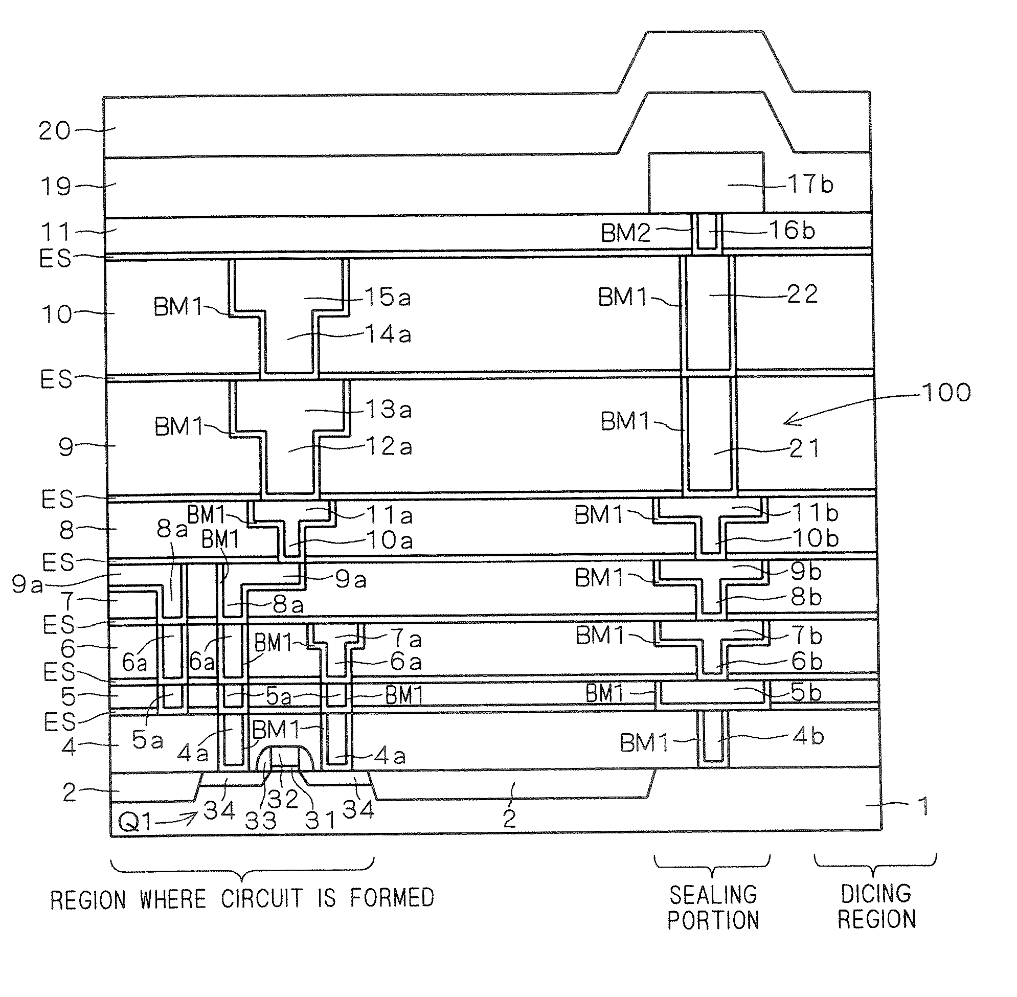
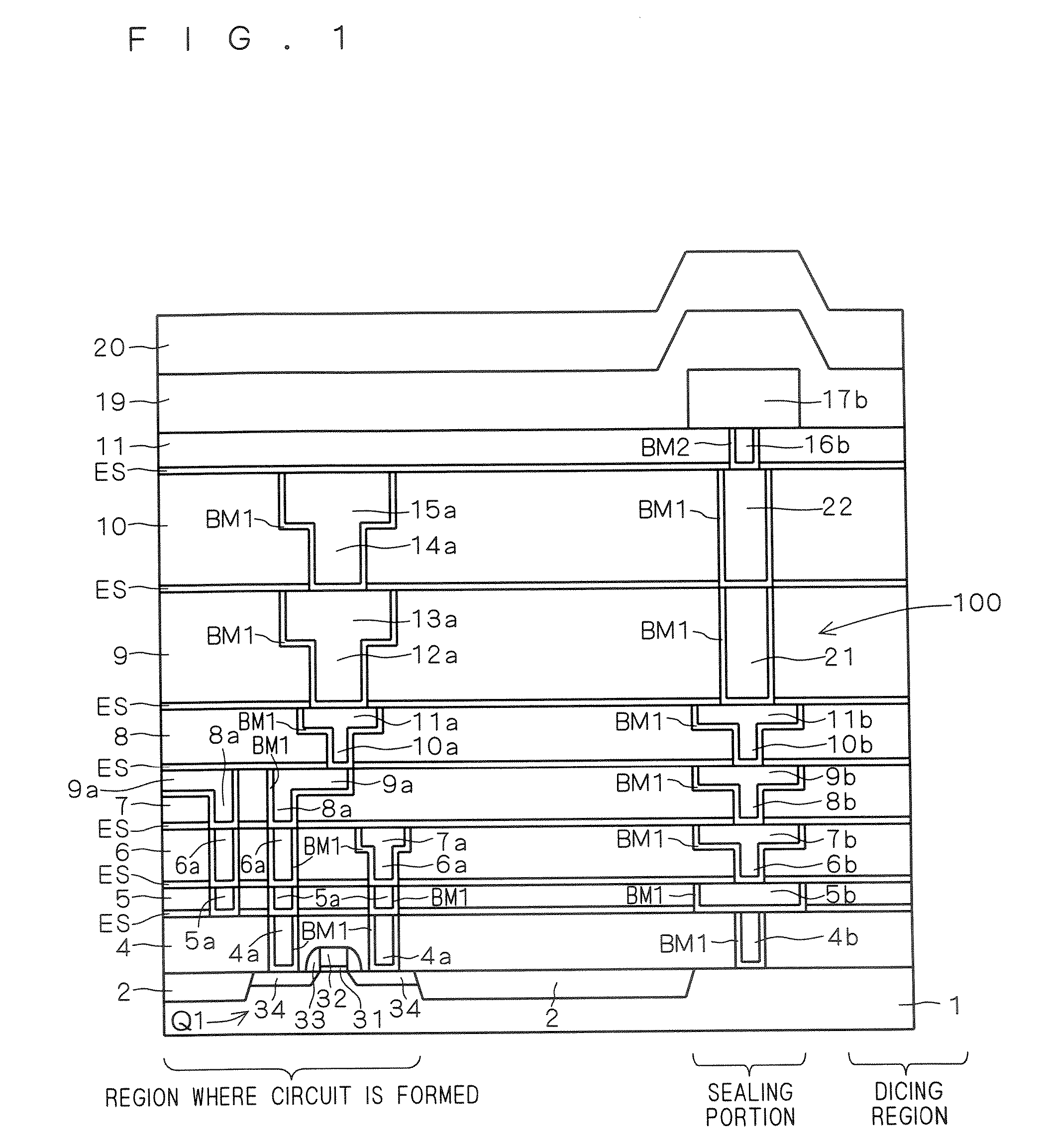
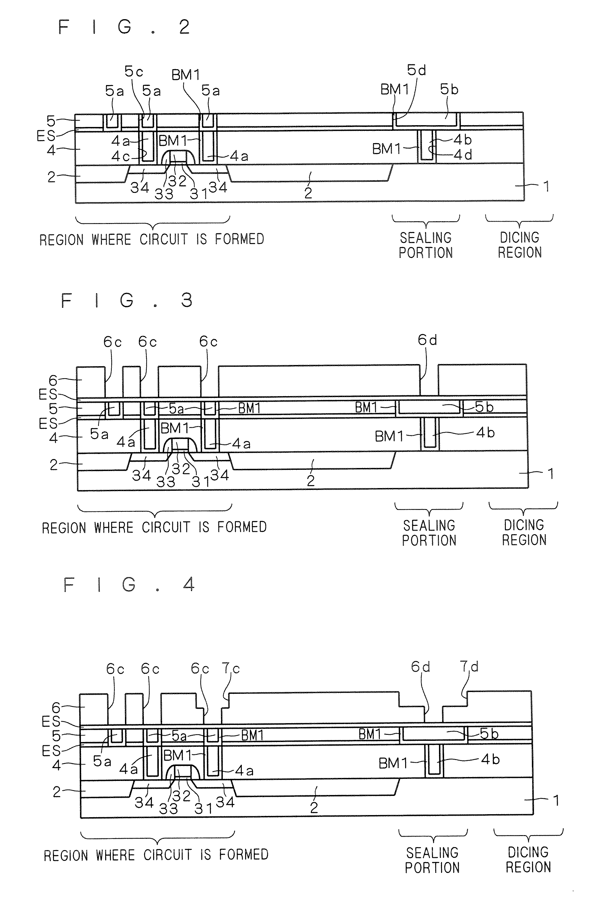
[0054]FIG. 1 is a cross sectional view showing a semiconductor device according to an embodiment of the present invention.

[0055]FIG. 1 shows a configuration where a MOS transistor Q1 is provided in an active region defined by an isolation insulating film 2 as an example of a semiconductor element which forms a semiconductor integrated circuit provided on a semiconductor substrate 1, for example a silicon substrate. In addition, a seal ring 100 is provided between the region where the circuit is formed on the semiconductor substrate 1 and the dicing region.

[0056] The MOS transistor Q1 is formed so as to have a gate electrode 32 which is provided on the semiconductor substrate 1 with a gate insulating film 31 in between, side wall insulating films 33 which are provided on the sides of the gate electrode 32, and source / drain layers 34 which are respectively provided on the surface of the semiconductor substrate 1, on both sides and the outside of the gate ele...


PUM


Abstract

A seal ring is provided between a region where a circuit is formed on a semiconductor substrate and a dicing region. The seal ring has a portion where sealing layers of which the cross sectional form is in T-shape are layered and a portion where sealing layers of which the cross sectional form is rectangular are layered.

Description

BACKGROUND OF THE INVENTION [0001] 1. Field of the Invention [0002] The present invention relates to a semiconductor device and a method of manufacture thereof, and in particular, to a semiconductor device having a seal ring provided so as to surround the periphery of a semiconductor integrated circuit, and a method of manufacture thereof. [0003] 2. Description of the Background Art [0004] In a manufacturing process for a semiconductor device, a semiconductor substrate is cut along dicing line portions, and thereby, is separated into individual LSI chips after a plurality of semiconductor elements have been formed on the semiconductor substrate. At this time, multiple interlayer insulating films layered during the process for forming the semiconductor elements are exposed from the cut section of the dicing line portions. [0005] These interlayer insulating films and interfaces between the interlayer insulating films become paths for moisture to penetrate, and there is a possibility t...

Claims


Application Information

Patent Timeline
Patent Type & Authority Applications(United States)
IPC IPC(8): H01L29/788
CPCH01L21/768H01L23/585H01L2924/0002H01L2924/00H01L21/28
Inventor MORIMOTO, NOBORUFUJISAWA, MASAHIKOKODAMA, DAISUKE
Owner RENESAS ELECTRONICS CORP
Why Eureka
Try Eureka