Color converting substrate, method for producing the same and light emitting device

a technology of color conversion substrate and color conversion substrate, which is applied in the manufacture of electrode systems, electric discharge tubes/lamps, and discharge tubes luminescnet screens, etc., can solve the problems of reduced red purity, impaired white balance, and decreased conversion efficiency into red light, and achieves excellent white balance and durability, high efficiency, and uniform emission

Inactive Publication Date: 2007-04-26
IDEMITSU KOSAN CO LTD
View PDF12 Cites 73 Cited by
  • Summary
  • Abstract
  • Description
  • Claims
  • Application Information

AI Technical Summary

Benefits of technology

[0035] According to the color conversion substrate of the invention, a multicolor emitting apparatus with excellent white balance and durability can be obtained.
[0036] According to the color conversion substrate of the invention, a white emitting apparatus with high efficiency and uniform emission can be obtained.

Problems solved by technology

However, since concentration quenching occurs due to an increase in the concentration of the fluorescent material, the conversion efficiency into red light is decreased and the red purity is decreased.
However, an emitting apparatus including a white emitting device and a color conversion substrate using organic fluorescent materials for a green fluorescent layer and a red fluorescent layer exhibits relatively weak blue emission, whereby the white balance is impaired.
However, it is difficult to adjust the emission color of the emitting device, since the device configuration becomes complicated and the drive characteristics (current-voltage-luminance characteristics) and durability (e.g. stability and high-temperature drive characteristics) of the device must be improved.
However, when using semiconductor nanocrystals of which the particle size must be strictly controlled as red and green fluorescent materials, the quality of the color conversion substrate may become unstable, or the cost of the color conversion substrate may be increased.
According to the emitting apparatus having this configuration, since the inorganic fluorescent material has a large particle size, light emitted from the emitting device and fluorescence undergo a significant scattering loss, whereby an efficient white emitting apparatus cannot be obtained.

Method used


Image

  • Color converting substrate, method for producing the same and light emitting device
  • Color converting substrate, method for producing the same and light emitting device
  • Color converting substrate, method for producing the same and light emitting device

Examples


first embodiment

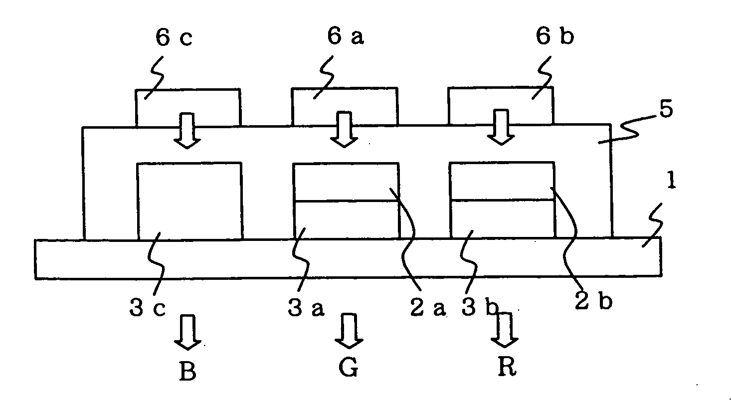
[0093]FIG. 6 is a schematic cross-sectional view showing a first embodiment of the emitting apparatus according to the invention.

[0094] This embodiment relates to a multicolor emitting apparatus in which a protective layer 5 is formed on the color conversion substrate according to the above-described second embodiment, and emitting devices 6a, 6b, and 6c are stacked at positions corresponding to the first fluorescent layer, the second fluorescent layer, and the blue color filter, respectively.

[0095] This emitting apparatus is a bottom emission type emitting apparatus in which the emitting devices are stacked on the color conversion substrate and light is outcoupled from the apparatus through the supporting substrate. This configuration facilitates alignment of the emitting devices (6a, 6b, 6c) and the color conversion substrate. Moreover, since only one substrate is necessary, the thickness and the weight of the emitting apparatus can be reduced.

second embodiment

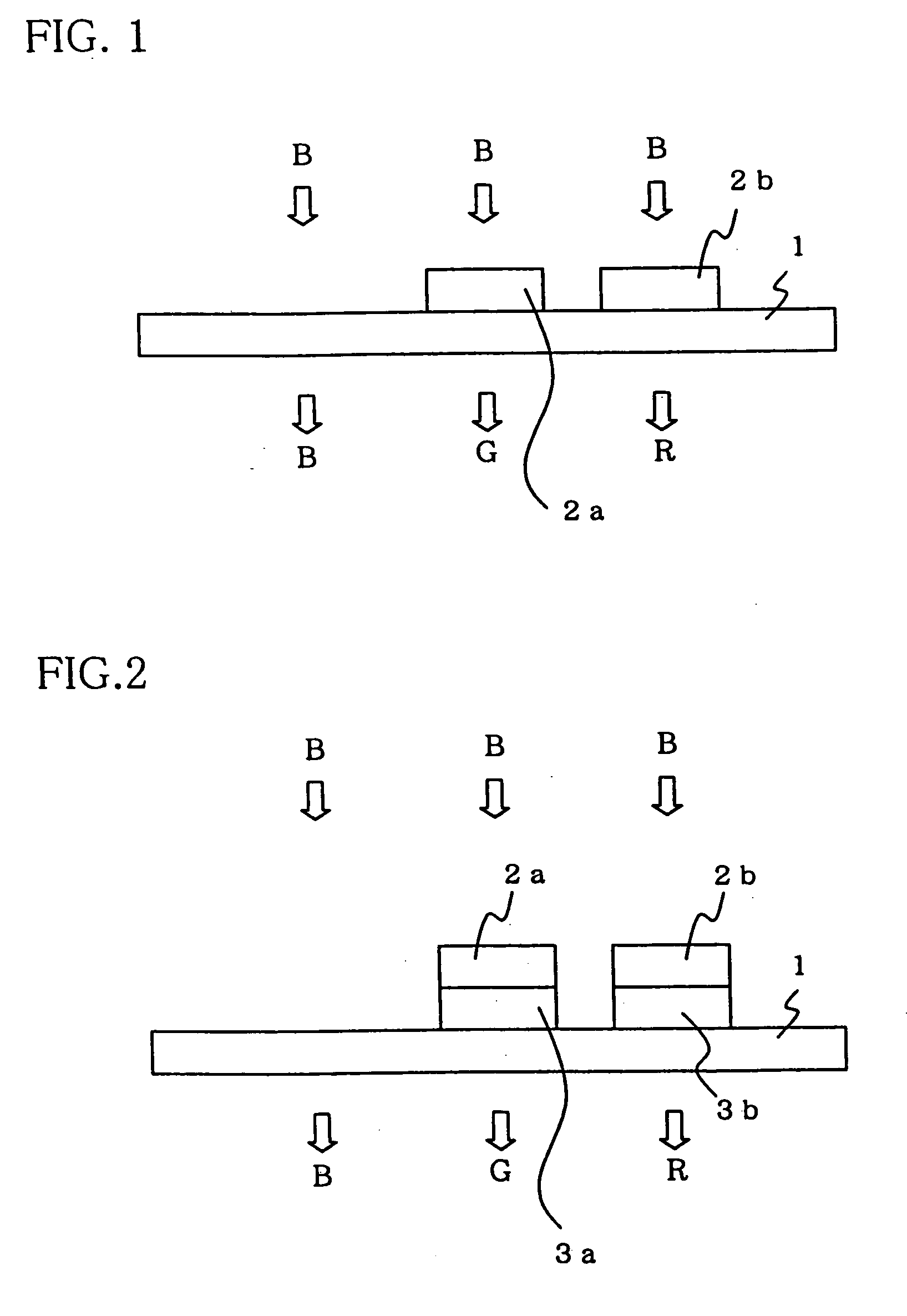
[0096]FIG. 7 is a schematic cross-sectional view showing a second embodiment of the emitting apparatus according to the invention.

[0097] This embodiment relates to a multicolor emitting apparatus in which the color conversion substrate 10 according to the above-described second embodiment and an emitting device substrate 20 in which the emitting devices (6a, 6b, 6c) are formed on a substrate 7 are bonded through an adhesive layer 8 so that the substrate 20 faces the substrate 10.

[0098] This emitting apparatus is a top emission type emitting apparatus in which the emitting devices face the color conversion substrate and light is outcoupled from the apparatus not through the substrate 7 on which the emitting devices are formed. According to this embodiment, since the color conversion substrate is separated from the emitting devices, adverse effects (e.g. unevenness of the substrate or movement of water from the fluorescent layers to the emitting devices) on the emitting devices due ...

third embodiment

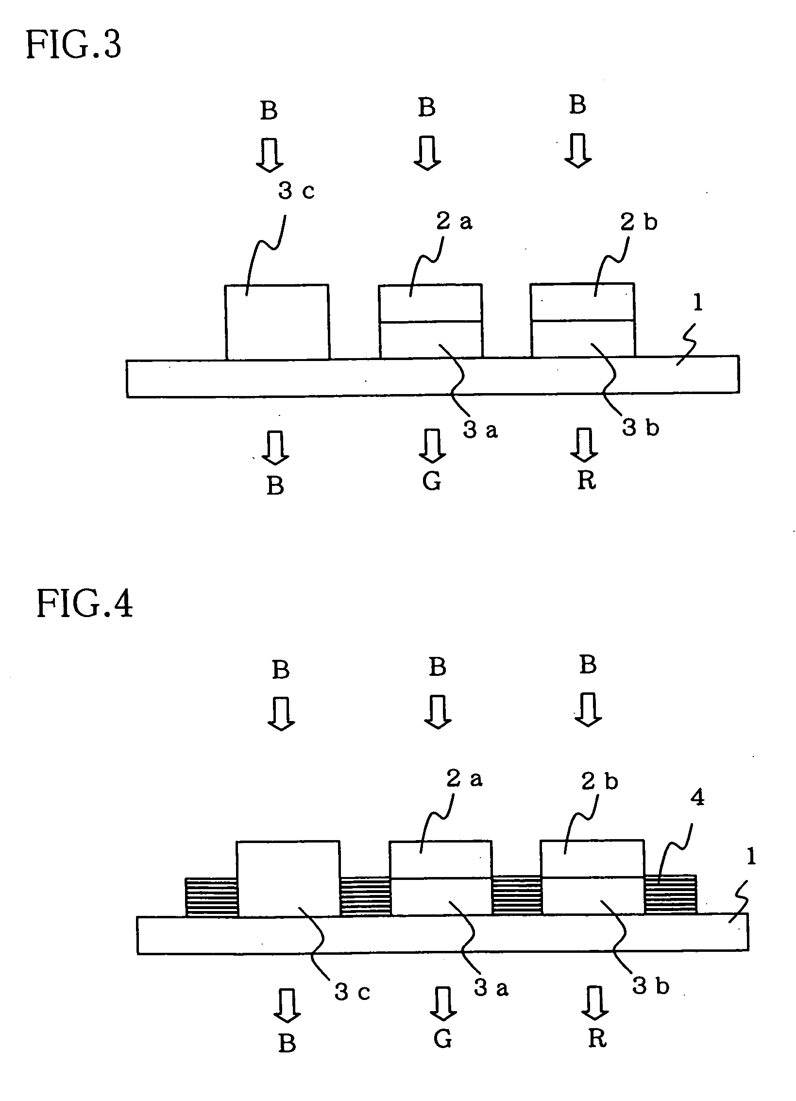
[0099]FIG. 8 is a schematic cross-sectional view showing a third embodiment of the emitting apparatus according to the invention.

[0100] This embodiment relates to a multicolor emitting apparatus in which the first emitting device 6a, the second emitting device 6b, and the third emitting device 6c are formed on the supporting substrate 1, and which includes first, second and third pixels 31, 32 and 33 on a passivation layer 9. In the first pixel 31, the first emitting device 6a, the first fluorescent layer 2a, and the color filter 3a are stacked in this order. In the second pixel 32, the second emitting device 6b, the first fluorescent layer 2b, and the color filter 3b are stacked in this order. In the third pixel 33, the third emitting device 6c and the color filter 3c are stacked.

[0101] According to the third embodiment, since the light emitted from the emitting device can be efficiently introduced into the fluorescent layer by directly disposing the fluorescent layer above the e...


PUM


Abstract

A color conversion substrate including a first fluorescent layer 2a emitting first fluorescence and a second fluorescent layer 2b emitting second fluorescence on a supporting substrate 1, and the first fluorescent layer 2a including an organic fluorescent material and the second fluorescent layer 2b comprising a semiconductor nanocrystal.

Description

TECHNICAL FIELD [0001] The invention relates to a color conversion substrate, a method for producing the color conversion substrate, and an emitting apparatus. More particularly, the invention relates to a color conversion substrate using a fluorescent layer including an organic fluorescent material and a fluorescent layer including a semiconductor nanocrystal. BACKGROUND ART [0002] A color conversion substrate which converts the wavelength of light emitted from a light source using a fluorescent material has been applied in various fields such as the electronic display field. [0003] For example, a technology has been disclosed which converts light emitted from a blue emitting device into green light and red light using fluorescent material layers to emit light of blue, green, and red (i.e. three primary colors), thereby achieving a full color display (see patent documents 1 to 3, for example). [0004] According to the above method, since a single-color emitting device can be used, i...

Claims


Application Information

Patent Timeline
Patent Type & Authority Applications(United States)
IPC IPC(8): H01J9/24H01J1/62
CPCB82Y20/00H01L27/322H10K59/38H10K71/236H10K85/621H10K85/6574H10K59/10H10K2101/27
Inventor EIDA, MITSURUHACHIYA, SATOSHIKATANO, JUNICHI
Owner IDEMITSU KOSAN CO LTD
Why Eureka
Try Eureka