Solid-state imaging apparatus and camera

a solid-state imaging and camera technology, applied in the field of solid-state imaging apparatuses and cameras, can solve the problems of pixel-to-pixel sensitivity variations and undesirable creation of extra space around a pixel, and achieve the effect of reducing the number of readout circuits, maximizing the area of the sensor in the pixel, and reducing extra space other than the sensor

Active Publication Date: 2007-04-26
SONY CORP
View PDF12 Cites 150 Cited by
  • Summary
  • Abstract
  • Description
  • Claims
  • Application Information

AI Technical Summary

Benefits of technology

[0017] In the invention, the number of readout circuits is reduced by employing the multi-pixel sharing structure, and the extra space other than the sensor is reduced by aligning the transistors forming the readout circuit in the region between the pixels. As a result, the area of the sensor in a pixel can be maximized.
[0018] The back-illuminated solid-state imaging apparatus having a multi-pixel sharing structure according to an embodiment of the invention can maximize the area of the sensor.

Problems solved by technology

However, in the front-illuminated solid-state imaging apparatus having a multi-pixel sharing structure, transistors forming the readout circuit may not be placed together because of layout constraints, but need to be placed apart from each other.
This undesirably creates an extra space around a pixel.
Partially expanding the area of the photodiode to effectively use this extra space causes the shape of each photodiode to be non-uniform, resulting in pixel-to-pixel sensitivity variations.
However, the fact is that there have been made few proposals to date for optimizing the layout of a back-illuminated solid-state imaging apparatus having a multi-pixel sharing structure.

Method used


Image

  • Solid-state imaging apparatus and camera
  • Solid-state imaging apparatus and camera
  • Solid-state imaging apparatus and camera

Examples


first embodiment

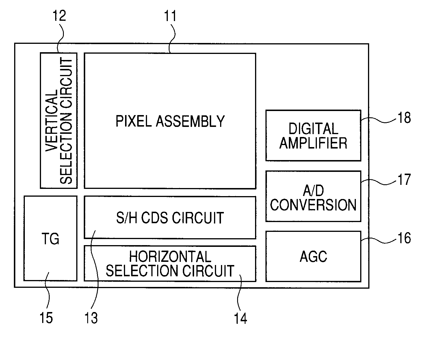
[0034]FIG. 1 shows a schematic block diagram of the solid-state imaging apparatus according to this embodiment.

[0035] The solid-state imaging apparatus includes an assembly of pixels 11 and peripheral circuits, which are mounted on a same semiconductor substrate. In this embodiment, the peripheral circuits include a vertical selection circuit 12, an S / H (Sample and Hold) CDS (Correlated Double Sampling) circuit 13, an horizontal selection circuit 14, a timing generator (TG) 15, an AGC (Automatic Gain Control) circuit 16, an A / D conversion circuit 17 and a digital amplifier 18.

[0036] The assembly of pixels 11 has a numerous unit pixels, which will be described later, arranged in a matrix, address lines (pixel selection lines) and the like on a row basis and signal lines and the like on a column basis.

[0037] The vertical selection circuit 12 sequentially selects pixels on a row basis and reads out a signal from each of the pixels on a pixel row basis to the S / H CDS circuit 13 via t...

second embodiment

[0082] In a second embodiment, a solid-state imaging apparatus with a four-pixel sharing structure arranged in another layout will be described.

[0083] FIGS. 8 to 10 show layouts of the assembly of pixels of the solid-state imaging apparatus according to this embodiment. FIG. 10 shows the final layout. In this embodiment, the explanation is divided using three figures for better understanding. That is, FIG. 8 shows a layout when a polysilicon electrode (gate electrode) layer is provided. FIG. 9 shows a layout when a first metal wiring layer is provided. FIG. 10 shows the final layout including a second metal wiring layer.

[0084] Description will be first made with reference to FIG. 8. The photodiodes 30 are formed in a matrix. Among the plurality of photodiodes 30, four photodiodes 31, 32, 33 and 34 arranged in the vertical and horizontal directions share one readout circuit 50.

[0085] The floating diffusion FD1 is disposed between the photodiode 31 and the photodiode 32 that is dia...

third embodiment

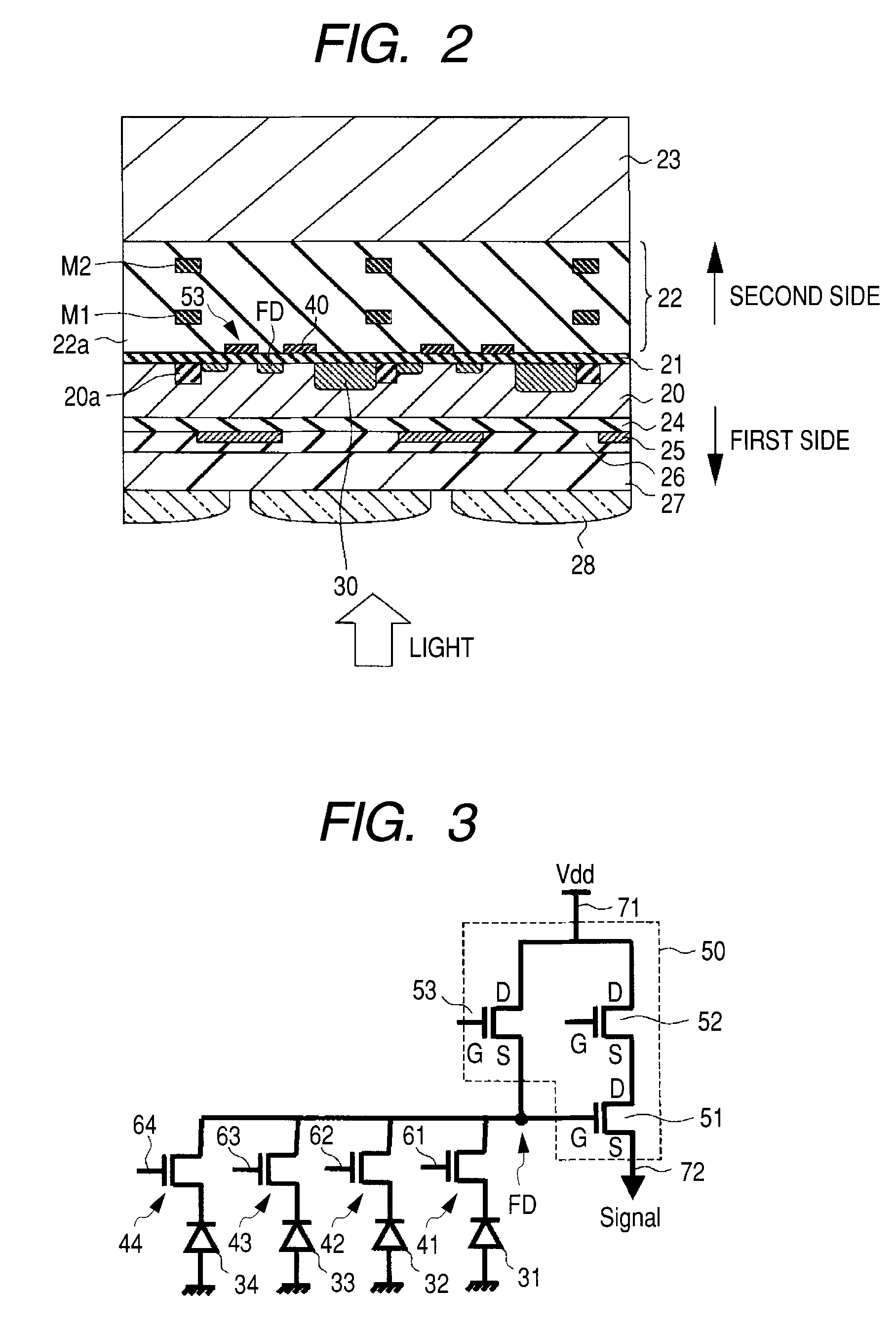
[0106] In a third embodiment, a solid-state imaging apparatus with a two-pixel sharing structure will be described. The circuit configuration of the assembly of pixels 11 in the case of the two-pixel sharing structure corresponds to the circuit diagram shown in FIG. 3 except that the photodiodes 33, 34, the transfer gates 43, 44 and the pixel selection lines 63, 64 are removed.

[0107] FIGS. 11 to 14 show layouts of the assembly of pixels of the solid-state imaging apparatus according to this embodiment. FIG. 14 shows the final layout. In this embodiment, the explanation is divided using four figures for better understanding. That is, FIG. 11 shows a layout when a polysilicon electrode (gate electrode) layer is provided. FIG. 12 shows a layout when a first metal wiring layer is provided. FIG. 13 shows a layout when a second metal wiring layer is provided. FIG. 14 shows the final layout including a third metal wiring layer.

[0108] Description will be first made with reference to FIG. ...


PUM


Abstract

A solid-state imaging apparatus includes a plurality of sensors that are formed on a substrate on a pixel basis and photoelectrically convert the light incident from a first surface side of the substrate, and a readout circuit that is formed on a second surface side of the substrate, which is the opposite side to the first surface side, and processes a signal from the plurality of sensors. The readout circuit includes a plurality of transistors and the transistors are disposed in a region between the pixels in an aligned manner.

Description

CROSS REFERENCES TO RELATED APPLICATIONS [0001] The present invention contains subject matter related to Japanese Patent Application JP 2005-307636 filed in the Japanese Patent Office on Oct. 21, 2005, the entire contents of which being incorporated herein by reference.BACKGROUND OF THE INVENTION [0002] 1. Field of the Invention [0003] The present invention relates to a solid-state imaging apparatus and a camera, and particularly to a back-illuminated solid-state imaging apparatus and a camera with the solid-state imaging apparatus. [0004] 2. Description of the Related Art [0005] As a solid-state imaging apparatus, an image sensor using a MOS (Metal Oxide Semiconductor) transistor (hereinafter referred to as a MOS-type solid-state imaging apparatus), which is a standard technology in IC manufacturing, has become widely used. The MOS-type solid-state imaging apparatus has an advantage in that it may not require a high drive voltage unlike a CCD (Charge Coupled Device) and it can be c...

Claims


Application Information

Patent Timeline
Patent Type & Authority Applications(United States)
IPC IPC(8): H04N5/335H01L27/146H04N5/369H04N5/374H04N5/376
CPCH01L27/14603H01L27/14609H01L27/14641H04N5/335H01L27/1464H01L27/14627H04N25/00H04N25/79H01L27/146
Inventor IWABUCHI, SHINKARASAWA, NOBUHIRO
Owner SONY CORP
Why Eureka
Try Eureka