Temperature controlled semiconductor processing chamber liner

a technology of semiconductor processing chamber and liner, which is applied in the direction of electromagnetic relay details, coatings, relays, etc., can solve the problems of releasing particles into the chamber environment, affecting the processing efficiency of semiconductors, so as to reduce the amount of material deposited, and reduce the effect of thermal cycling

Inactive Publication Date: 2007-04-26
APPLIED MATERIALS INC
View PDF17 Cites 9 Cited by
  • Summary
  • Abstract
  • Description
  • Claims
  • Application Information

AI Technical Summary

Benefits of technology

[0016] The thermally controlled chamber liner maintains a predetermined temperature by running coolant fluid or heating fluid from a fluid supply through the fluid passages. By maintaining a predetermined temperature, the chamber liner manages the deposition of films upon the chamber liner by both minimizing the amount of material deposited upon the liner and maintaining the liner at a uniform temperature with minimal thermal cycling. The controlled temperature of the liner surface discourages deposition, and the substantially constant temperature (i.e., limited temperature cycling) reduces stress formation in films deposited on the liner, thus increasing service life of the liner while minimizing film fracture and the associated particulate generation.

Problems solved by technology

Some of this material may deposit upon various tool components before it can be exhausted from the processing chamber resulting in a buildup of material on these components.
Eventually, the stresses can cause the films to crack, consequently releasing particles into the chamber environment.
These film particles may impinge upon the wafer surface, typically creating a defect in the circuit structure on the wafer.
Due to this problem, the chamber must undergo periodic cleaning cycles to remove these films resulting in tool downtime and diminished wafer throughput.
However, in chambers using chamber liners, such temperature control is difficult and unpredictable.
Additionally, as the surface topography of the liner and mating chamber surface is irregular (on a microscopic level), the heat transfer between liners and the chamber can be less than desirable and irreproducible.
Such thermal inconsistencies aggravate the stresses within the deposited film layer, accelerating the film cracking and particulate generation process.
This increased preventative maintenance activity ultimately decreases tool capacity and wafer throughput.
Additionally, new processing regimes utilizing increased RF power further exasperate liner thermal differentials.

Method used


Image

  • Temperature controlled semiconductor processing chamber liner
  • Temperature controlled semiconductor processing chamber liner
  • Temperature controlled semiconductor processing chamber liner

Examples


Embodiment Construction

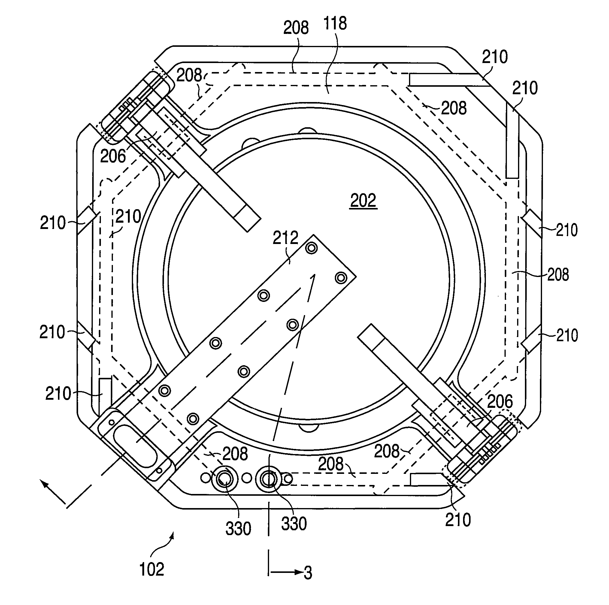
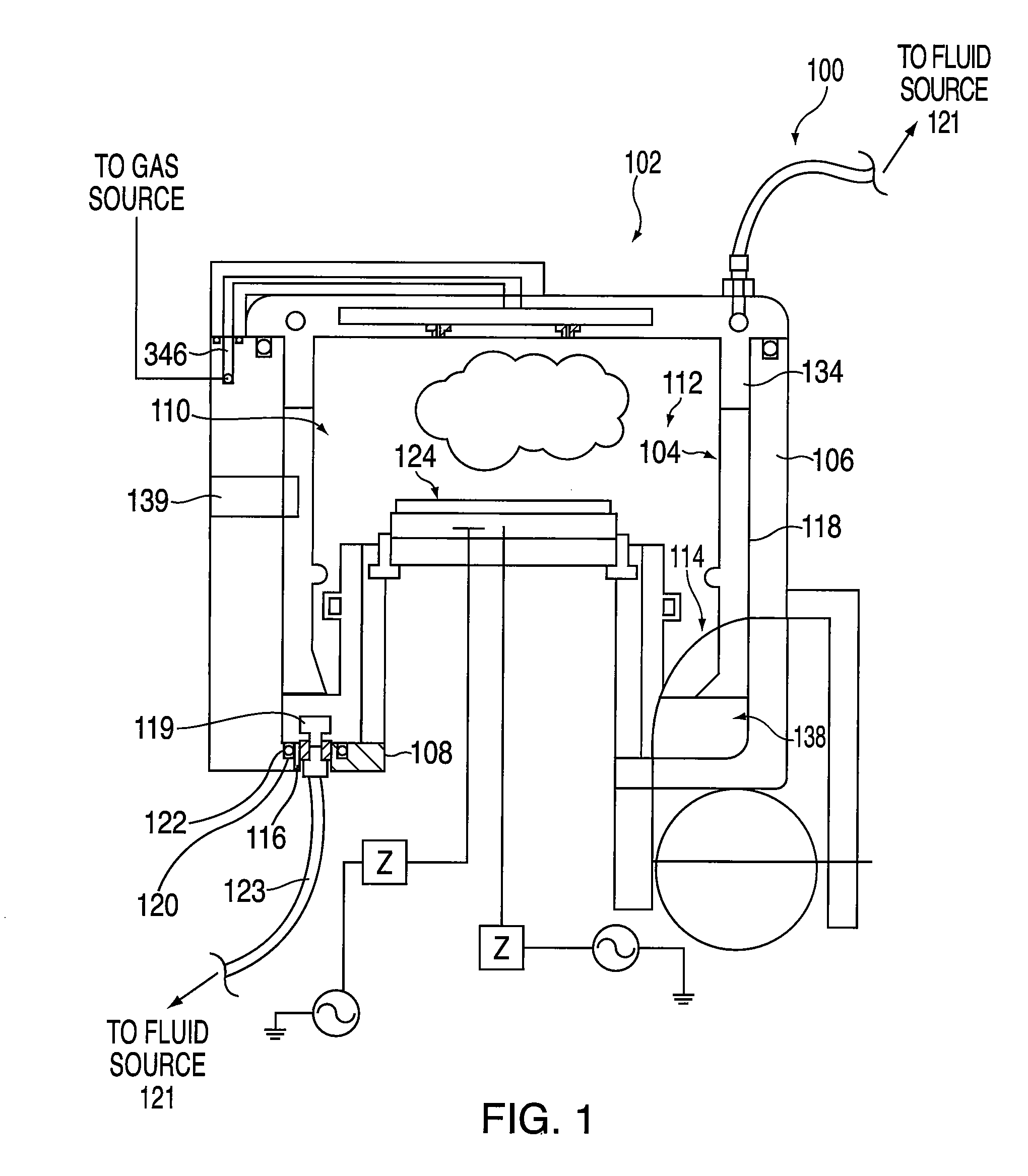
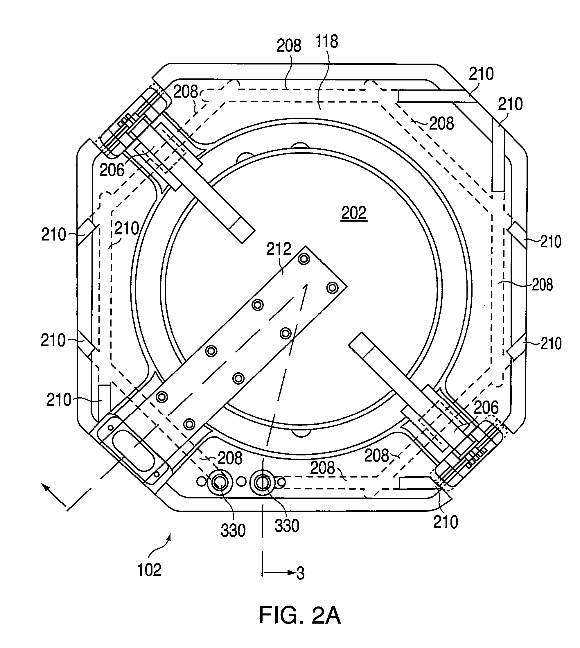
[0030] The present invention generally provides a temperature controlled chamber component, such as a chamber liner, for use in a substrate processing system. The invention also provides methods for controlling the temperature of chamber components, including the chamber liner, and thus, substantially minimizes the amount of deposition on these chamber components. The chamber liner comprises a first liner and / or a second liner, which may be utilized individually or in concert.

[0031] The invention will be described below initially with reference to embodiments having both a first liner and a second liner disposed within an etch chamber. However, it should be understood that the description applies to other chamber configurations such as physical vapor deposition chambers and chemical vapor deposition chambers in which the deposition of material upon chamber components is unwanted. It is to be understood that the invention can be utilized in other chamber configurations benefiting fr...


PUM

PropertyMeasurementUnit
temperatureaaaaaaaaaa
flatnessaaaaaaaaaa
diameteraaaaaaaaaa

Abstract

A thermally controlled chamber liner comprising a passage having an inlet and outlet adapted to flow a fluid through the one or more fluid passages formed at least partially therein. The chamber liner may comprise a first liner, a second liner or both a first liner and a second liner. The thermally controlled chamber liner maintains a predetermined temperature by running fluid from a temperature controlled, fluid source through the fluid passages. By maintaining a predetermined temperature, deposition of films on the chamber liner is discouraged and particulate generation due to stress cracking of deposited films is minimized.

Description

CROSS-REFERENCE TO RELATED APPLICATIONS [0001] This application is a continuation of co-pending U.S. patent application Ser. No. 10 / 055,310 (Attorney Docket No. 004150.D1), filed Jan. 22, 2002, which is a divisional of U.S. patent application Ser. No. 09 / 519,719 (Attorney Docket No. 004150), filed Mar. 7, 2000, both of which are hereby incorporated by reference herein in their entirety.BACKGROUND OF THE INVENTION [0002] 1. Field of Invention [0003] The present invention relates generally to a semiconductor wafer processing apparatus. More specifically, the invention relates to an apparatus for providing a temperature controlled chamber liner. [0004] 2. Background of the Related Art [0005] In semiconductor wafer processing, minimizing particulate contamination of a substrate is a critical process parameter. Tool materials are selected and processes are performed in reduced atmospheres to assist in reducing and managing particles that may be present and / or generated in the processing ...

Claims


Application Information

Patent Timeline
Patent Type & Authority Applications(United States)
IPC IPC(8): H01H47/26H01H47/32H01H50/12C23C16/44C23C16/455H01J37/32
CPCC23C16/4401C23C16/4411C23C16/45563H01J37/32522H01J37/32623H01J37/32633H01J2237/2001
Inventor NOORBAKHSH, HAMIDSALIMIAN, SIAMAKLUSCHER, PAULCARDUCCI, JAMES D.LEE, EVANSVAIDYA, KAUSHIKSHAN, HONGQINGWELCH, MICHAEL D.
Owner APPLIED MATERIALS INC
Why Eureka
Try Eureka