Semiconductor laser device and method for manufacturing the same semiconductor laser device

a semiconductor laser and laser device technology, applied in semiconductor lasers, laser cooling arrangements, laser details, etc., can solve the problems of oxidation deformation and radiative recombination centers to deteriorate the device, and achieve the effect of lowering the current injection efficiency and preventing the deterioration of the device due to the oxidation of an active layer on the mesa side surfa

Inactive Publication Date: 2007-04-26
MITSUBISHI ELECTRIC CORP
View PDF13 Cites 8 Cited by
  • Summary
  • Abstract
  • Description
  • Claims
  • Application Information

AI Technical Summary

Benefits of technology

[0017] According to the present invention, in a semiconductor laser device using an AlGaInAs-based material and a method for manufacturing such a semiconductor laser device, the deterioration of the device due to the oxidation of an active layer on a mesa side surface can be prevented. The lowering of current injection efficiency by an ineffective current path that does not pass through an active layer can also be suppressed.

Problems solved by technology

If electric current is injected into the active layer of such a semiconductor laser, the defects formed by the oxides of Al create non radiative recombination centers to deteriorate the device.

Method used


Image

  • Semiconductor laser device and method for manufacturing the same semiconductor laser device
  • Semiconductor laser device and method for manufacturing the same semiconductor laser device
  • Semiconductor laser device and method for manufacturing the same semiconductor laser device

Examples


embodiment

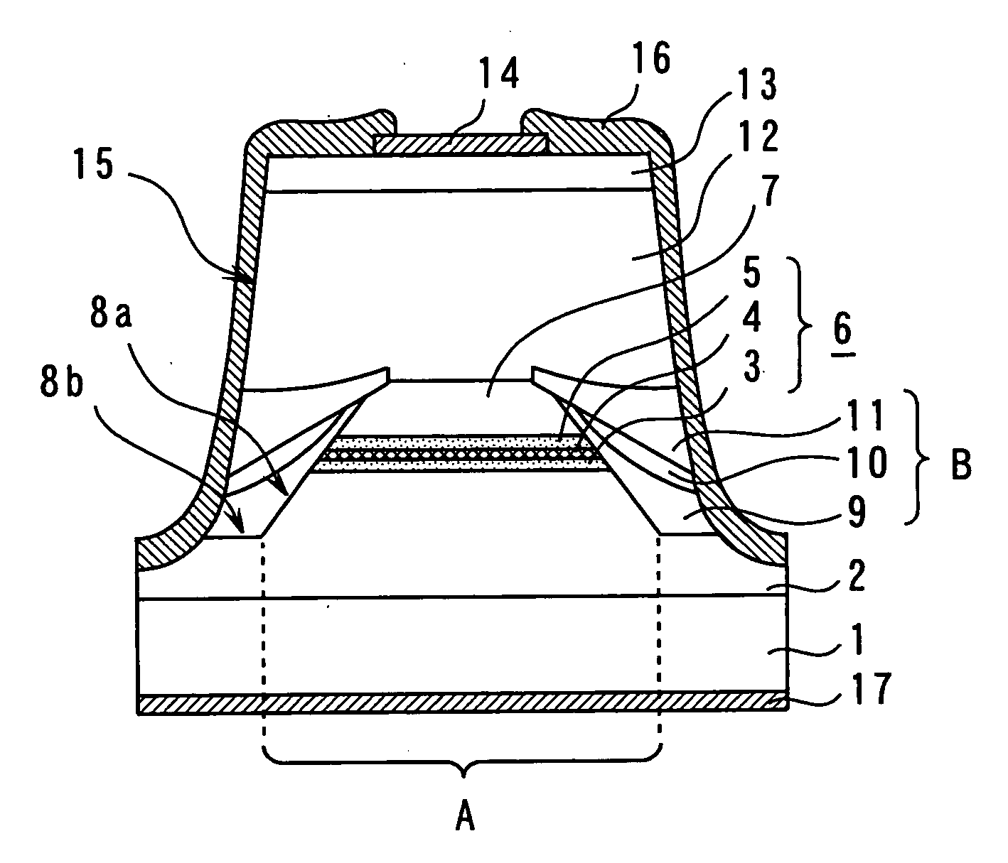
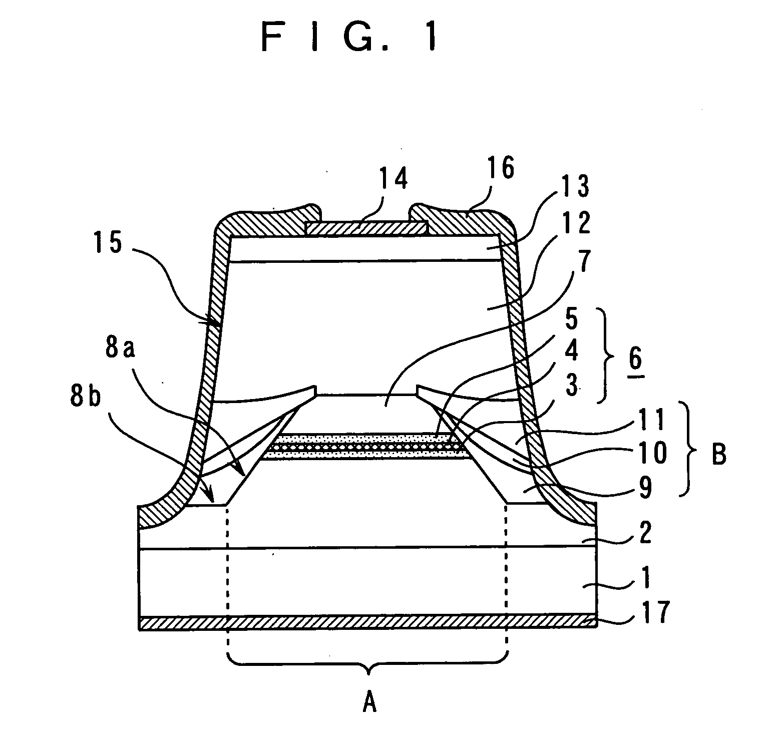
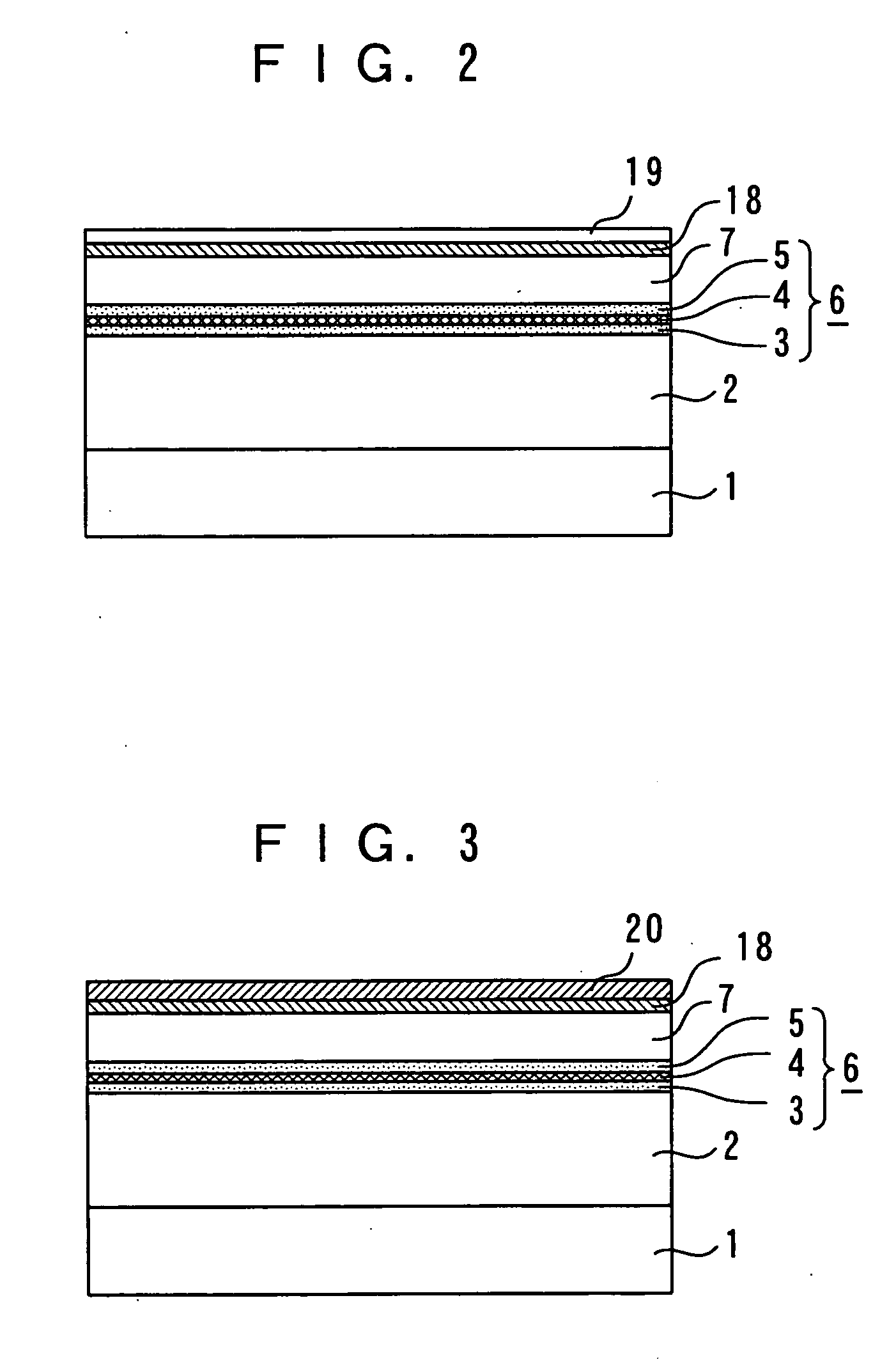
[0022] The structure of a semiconductor laser device according to this embodiment is shown in FIG. 1. The semiconductor laser device is formed on a p-type InP substrate 1. A p-type InP clad layer 2 is formed thereon. On the p-type InP clad layer 2, a lower light confinement layer 3, a multiple quantum well (hereafter abbreviated as “MQW”) active layer 4, and an upper light confinement layer 5 are laminated in the order from the bottom (hereafter, the structure formed by laminating these layers is referred to as a “laminated structure 6”). By injecting electrons and holes into the MQW active layer 4, laser beams can be generated. An n-type InP clad layer 7 is formed on the laminated structure 6.

[0023] A ridge part A is formed of the p-type InP clad layer 2, the laminated structure 6, and the n-type InP clad layer 7. A (111) B surface is exposed on the side surface of the ridge part A. The ridge part A has a sequentially tapered mesa shape wherein the side thereof has a predetermined...


PUM


Abstract

A current blocking structure of a semiconductor laser includes a p-type InP buried layer, an n-type InP current blocking layer, and a p-type InP current blocking layer laminated along the mesa side surface of a ridge. In the structure, an upper end part of the n-type InP current blocking layer is covered with the p-type InP buried layer and the p-type InP current blocking layer. The n-type InP current blocking layer is prevented from contacting n-type and p-type InP cladding layers. Creation of an ineffective current path from one of the n-type InP cladding layers through the n-type InP current blocking layer to a p-type InP cladding layer of the semiconductor laser is prevented.

Description

BACKGROUND OF THE INVENTION [0001] 1. Field of the Invention [0002] The present invention relates to a semiconductor laser device and method for manufacturing the same, and more specifically to a buried semiconductor laser device and method for manufacturing the same. [0003] 2. Background Art [0004] With the expansion of optical fiber communications network in recent years, demands for semiconductor laser devices that enable high-speed operation at high temperatures have been increasing. As a product to realize such demands, a semiconductor laser device using an AlGaInAs-based material for an active layer is attracting attention. [0005] Since Al-containing semiconductor materials are easily oxidized, oxides of Al are easily formed in such semiconductor materials. If electric current is injected into the active layer of such a semiconductor laser, the defects formed by the oxides of Al create non radiative recombination centers to deteriorate the device. Therefore, a semiconductor la...

Claims


Application Information

Patent Timeline
Patent Type & Authority Applications(United States)
IPC IPC(8): H01S5/00H01S3/04
CPCH01S5/2227H01S5/227H01S5/2275
Inventor WATATANI, CHIKARA
Owner MITSUBISHI ELECTRIC CORP
Why Eureka
Try Eureka