
Semiconductor device and method for fabricating the same

a technology of semiconductor devices and semiconductors, applied in the direction of resistors, diodes, electrical equipment, etc., can solve the problems of increasing the electrical thickness of the gate insulating film, hindering the enhancement of the performance of the fet, and increasing the circuit area, so as to reduce the circuit area and prevent the variation of electrical characteristics

Inactive Publication Date: 2007-04-26
PANASONIC CORP
View PDF4 Cites 24 Cited by
  • Summary
  • Abstract
  • Description
  • Claims
  • Application Information

AI Technical Summary

Benefits of technology

[0017] It is therefore an object of the present invention to prevent metal diffusion in a FUSI structure having different metal contents, especially in an integrated gate electrode.
[0049] As described above, with the semiconductor devices and the methods for fabricating the devices according to the present invention, metal diffusion occurring in a FUSI structure (especially an integrated gate electrode) having different metal contents is prevented or suppressed, and occurrence of an intermediate phase film due to metal diffusion is suppressed. As a result, the circuit area is reduced and variation in electrical characteristics is prevented.

Problems solved by technology

However, it is generally impossible to prevent depletion from being formed in polysilicon used for the gate electrode even by impurity implantation, resulting in that this depletion causes the electrical thickness of the gate insulating film to increase.
This hinders enhancement of performance of an FET.
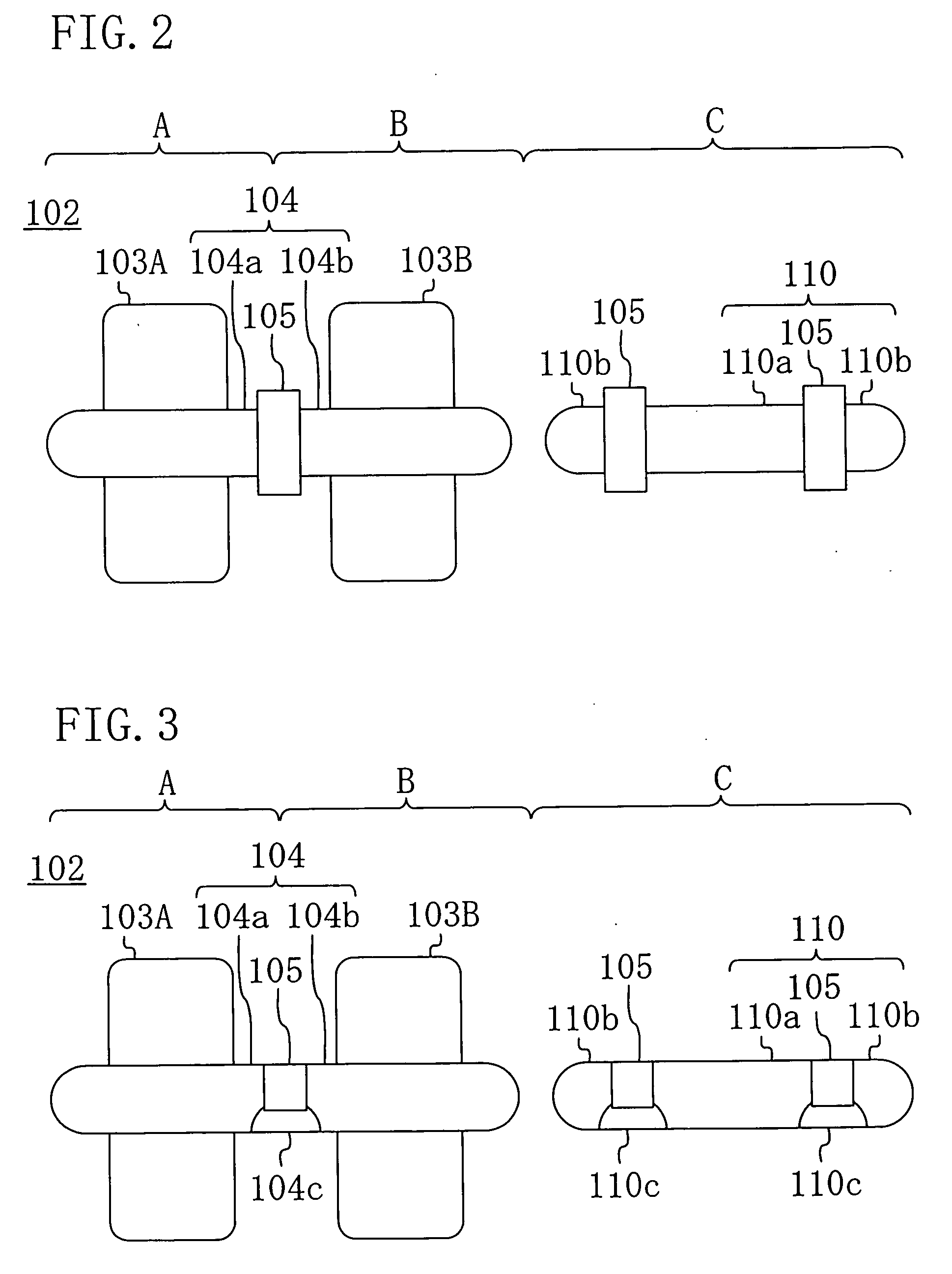
To avoid the variation of the threshold voltages caused by Ni diffusion, it is necessary to separate the first gate electrode 14a in the n-FET region A and the second gate electrode 14b in the p-FET region B and connect these electrodes through interconnection or to keep a sufficient distance between the n-FET region A and the p-FET region B. These methods have another problem that the circuit area increases.
With respect to the resistor 20, variation of the intermediate phase films 20c occurs among the resistors 20, thus making it difficult to obtain a desired resistance value.

Method used


Image

  • Semiconductor device and method for fabricating the same
  • Semiconductor device and method for fabricating the same
  • Semiconductor device and method for fabricating the same

Examples


embodiment 1

[0086] A first embodiment of the present invention will be described with reference to the drawings.

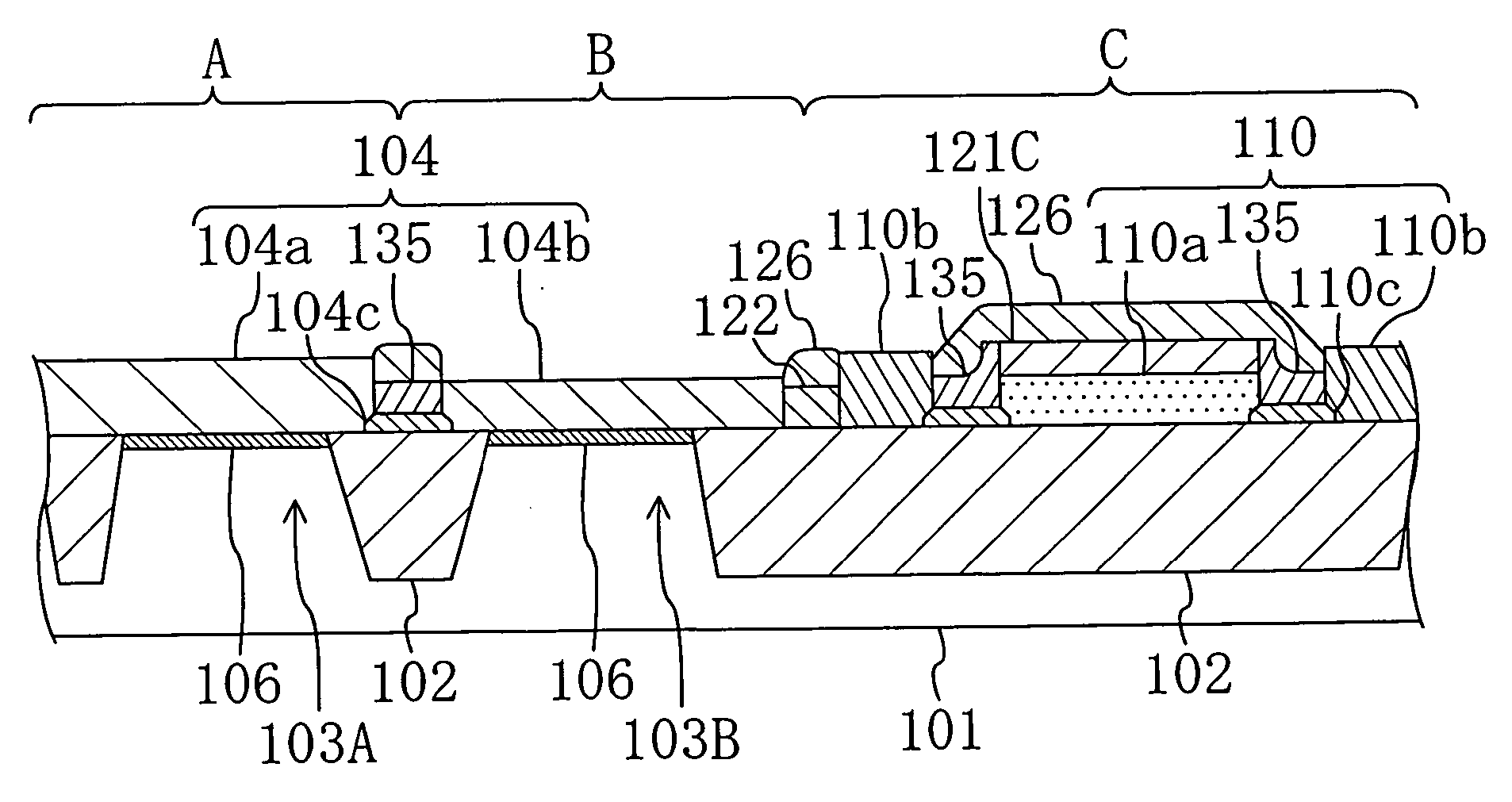
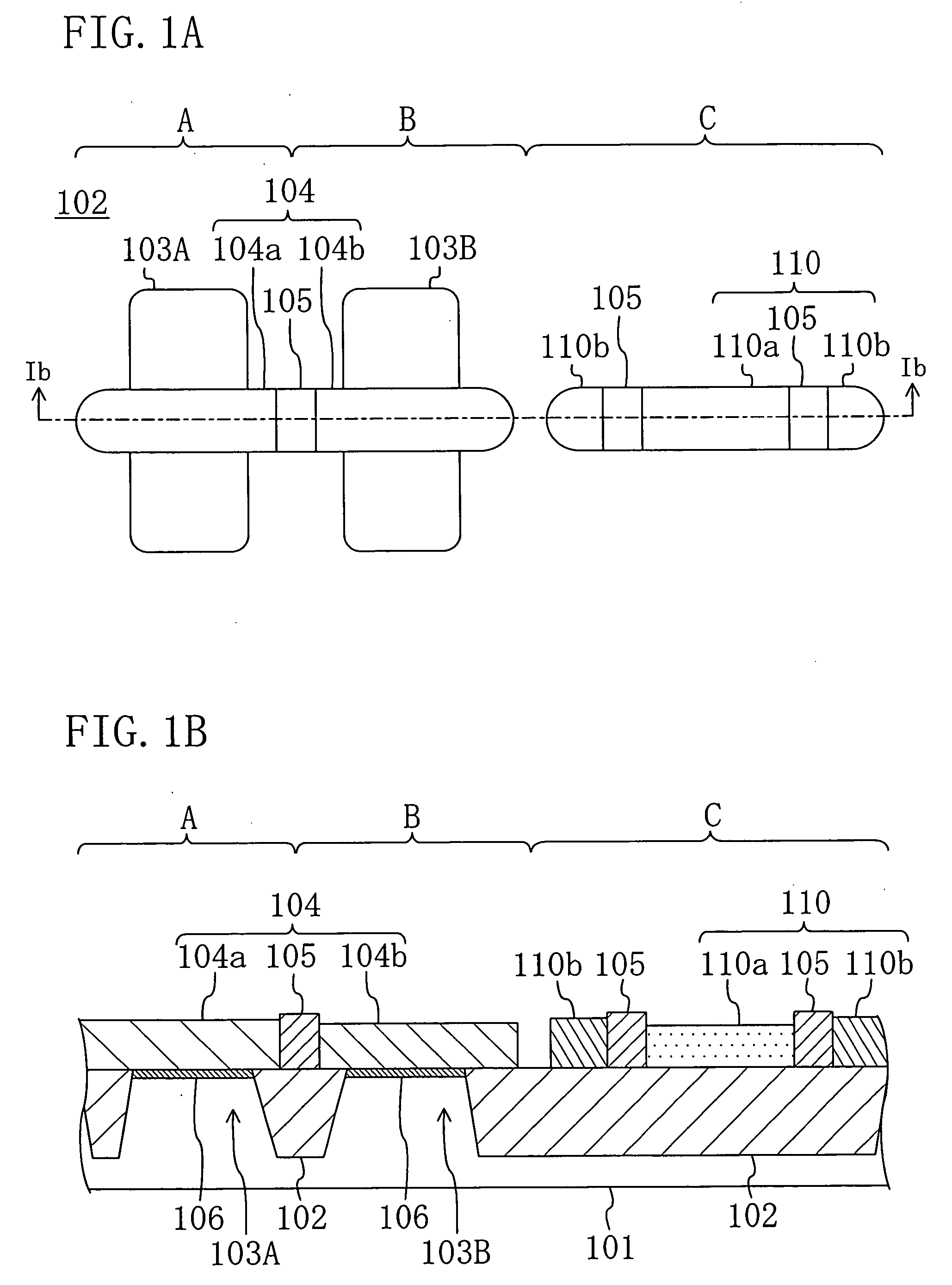
[0087]FIGS. 1A and 1B illustrate a semiconductor device according to the first embodiment. FIG. 1A is a plan view and FIG. 1B is a cross-sectional view taken along the line Ib-Ib in FIG. 1A. As illustrated in FIGS. 1A and 1B, the principal surface of a semiconductor substrate 101 made of, for example, silicon is partitioned into an n-FET region A, a p-FET region B and a resistor region C by an isolation region 102 of shallow trench isolation (STI).

[0088] An n-type active region 103A and a p-type active region 103B are formed in the respective n- and p-FET regions A and B. The n-type active region 103A and the p-type active region 103B are spaced out with their long sides (of rectangles) facing each other in plan view. A common gate electrode 104 is formed over the n-type active region 103A and the p-type active region 103B with a gate insulating film 106 of, for example, hafnium oxi...

embodiment 2

[0117] Hereinafter, a second embodiment of the present invention will be described with reference to the drawings.

[0118]FIGS. 16A and 16B illustrate a semiconductor device according to the second embodiment. FIG. 16A is a plan view and FIG. 16B is a cross-sectional view taken along the line XVIb-XVIb in FIG. 16A. In FIGS. 16A and 16B, components also shown in FIGS. 1A and 1B are denoted by the same reference numerals, and description thereof will be omitted.

[0119] As illustrated in FIGS. 16A and 16B, the second embodiment is different from the first embodiment in that an insulating material is used for diffusion preventing films 135. In this manner, if the diffusion preventing films 135 are made of silicon dioxide (SiO2), for example, increase in number of process steps is suppressed, as compared to cases of using other materials.

[0120] In addition, as illustrated in FIG. 16B, in the second embodiment, the diffusion preventing films 135 are made of an insulating material, so that...

embodiment 3

[0142] Hereinafter, a third embodiment of the present invention will be described with reference to the drawings.

[0143]FIGS. 26A and 26B illustrate a semiconductor device according to the third embodiment. FIG. 26A is a plan view and FIG. 26B is a cross-sectional view taken along the line XXVIb-XXVIb in FIG. 26A. In FIGS. 26A and 26B, components also shown in FIGS. 16A and 16B are denoted by the same reference numerals, and description thereof will be omitted.

[0144] As illustrated in FIGS. 26A and 26B, in the third embodiment, no diffusion preventing film 135 is provided in a connecting portion of a common gate electrode 104, and an intermediate phase film 104c thinner than gate electrodes 104a and 104b is left on the bottom of a first opening 120a. No diffusion preventing film 135 is also provided in a portion connecting a resistor body 110a and a contact region 110b in a resistor 110, and an intermediate phase film 110c thinner than the resistor body 110a and the contact region ...


PUM


Abstract

A semiconductor device includes a first field-effect transistor including a first gate electrode and a second field-effect transistor including a second gate electrode. The first gate electrode and the second gate electrode are integrated using a connecting portion and are fully silicided with a metal in such a manner that the fist and second gate electrodes have different metal contents. A diffusion preventing film for preventing the metal from diffusing between the first and second gate electrodes is formed in at least a portion of the connecting portion.

Description

CROSS-REFERENCE TO RELATED APPLICATION [0001] The disclosure of Japanese Patent Application No. 2005-311552 filed in Japan on Oct. 26, 2005 including specification, drawings and claims is incorporated herein by reference in its entirety. BACKGROUND OF THE INVENTION [0002] The present invention relates to semiconductor devices and methods for fabricating the devices, and particularly relates to semiconductor devices including field-effect transistors with fully-silicided (FUSI) structures and methods for fabricating the devices. [0003] The integration degree of semiconductor elements integrated in a semiconductor integrated circuit device has increased to date. For example, a technique for miniaturizing a gate electrode of a metal-insulator-semiconductor (MIS) field-effect transistor (FET) and reducing the electrical thickness of a gate insulating film by using a material with a high dielectric constant as an insulating material of a gate insulating film is being used. However, it is...

Claims


Application Information

Patent Timeline
Patent Type & Authority Applications(United States)
IPC IPC(8): H01L21/8238H01L21/336
CPCH01L21/823835H01L21/823842H01L21/823871H01L27/0629H01L28/20
Inventor KUDO, CHIAKIOGAWA, HISASHI
Owner PANASONIC CORP
Learn More