

Apparatus for manufacturing semiconductor device with pump unit and method for cleaning the pump unit
- Summary
- Abstract
- Description
- Claims
- Application Information
AI Technical Summary
Benefits of technology
Problems solved by technology
Method used
Image

Examples
Embodiment Construction
[0031] Hereinafter, exemplary embodiments of the present invention will be described in detail with reference to the accompanying drawings. In the drawings, the size and relative sizes of layers and regions may be exaggerated for clarity.
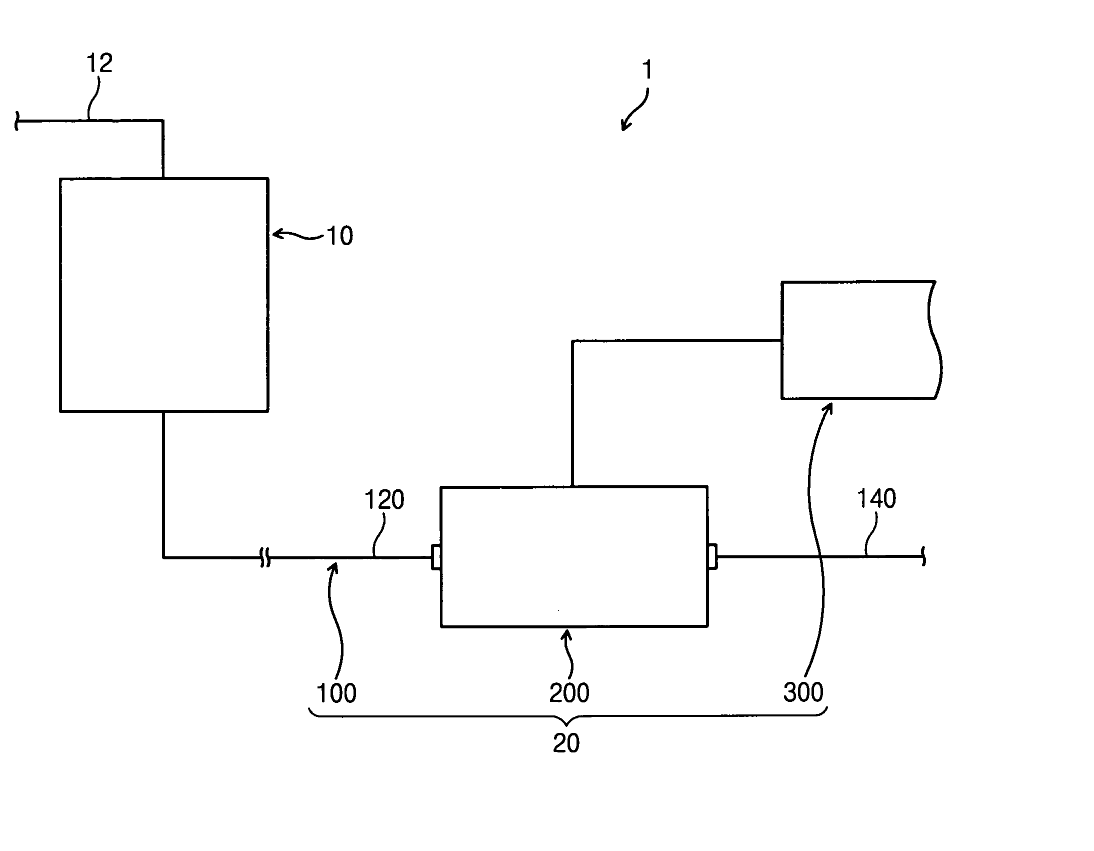
[0032]FIG. 1 is a schematic view of an apparatus for manufacturing a semiconductor device according to an exemplary embodiment of the present invention. Referring to FIG. 1, a semiconductor device manufacturing apparatus 1 includes a chamber 10 and an exhaust system 20. The chamber 10 is configured with a substrate support for supporting a semiconductor substrate such as a wafer (not shown). A process gas that will be deposited on the wafer is supplied into the chamber 10 through a gas supply pipe 12. The exhaust system 20 is coupled with the chamber 10. The exhaust system 20 is operable to maintain an internal pressure of the chamber 10 at a process pressure and exhaust reaction byproducts out of the chamber 10.
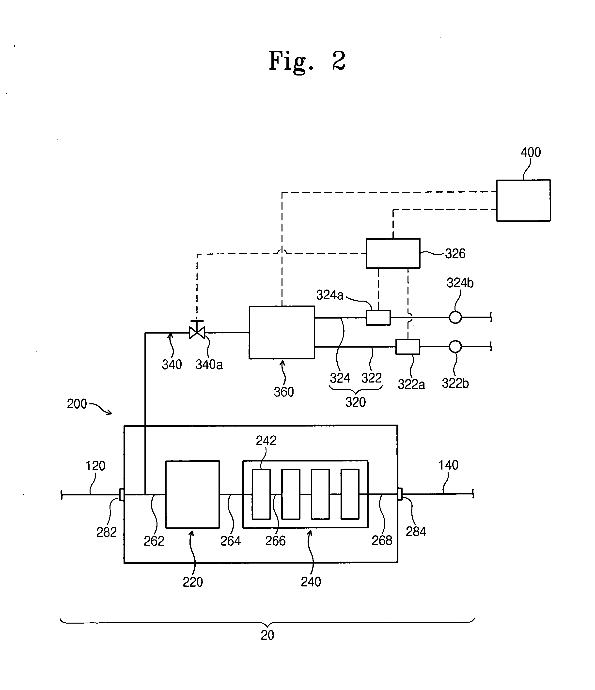
[0033] The exhaust system 20 of FIG...
PUM
| Property | Measurement | Unit |
|---|---|---|
| Time | aaaaa | aaaaa |
| Power | aaaaa | aaaaa |
| Flow rate | aaaaa | aaaaa |
Abstract
Description
Claims
Application Information