Semiconductor device and method for fabricating the same

Inactive Publication Date: 2007-05-03
PANASONIC CORP
0 Cites 33 Cited by

AI-Extracted Technical Summary

Problems solved by technology

However, after a known semiconductor device including a shared contact plug was studied in various manners, the present inventors found the following problems.
However, ...

Benefits of technology

[0010] However, after a known semiconductor device including a shared contact plug was studied in various manners, the present inventors found the following problems. With further miniaturization of gate electrodes, the structure of a semiconductor device in which a silicide laye...

Abstract

A semiconductor device includes a fully silicided first gate interconnect formed on a semiconductor substrate, a first sidewall formed on a side of the first gate interconnect, and impurity diffusion layers formed in an active region of the semiconductor substrate. A shared contact plug is formed in an interlayer dielectric formed on the semiconductor substrate so as to be connected to the first gate interconnect and associated one of the impurity diffusion layers. The first gate interconnect is formed, at its part connected to the shared contact plug, with a projection part projecting beyond the first sidewall.

Application Domain

Technology Topic

PhysicsImpurity diffusion +3

Image

  • Semiconductor device and method for fabricating the same
  • Semiconductor device and method for fabricating the same
  • Semiconductor device and method for fabricating the same

Examples

  • Experimental program(2)

Example

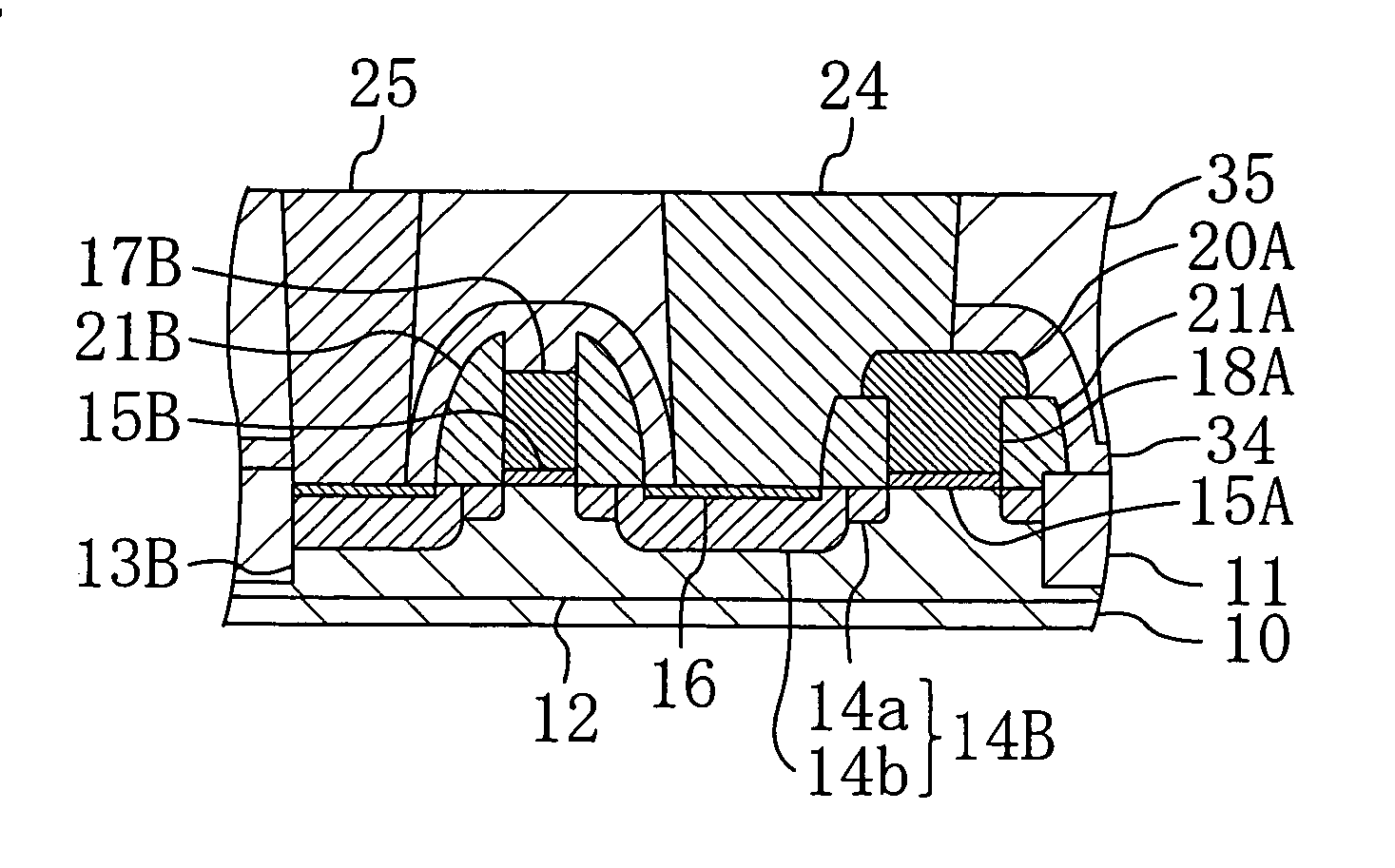
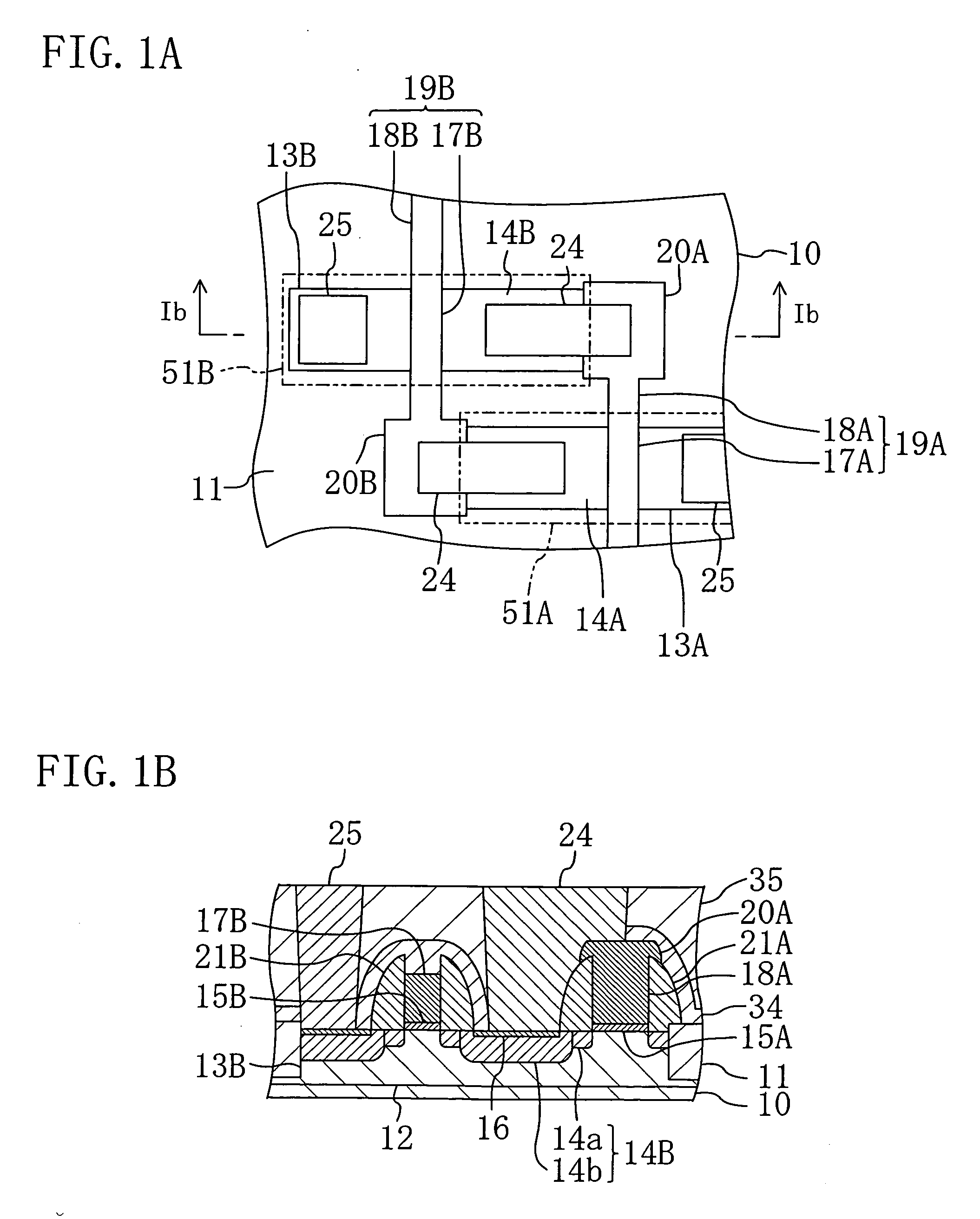
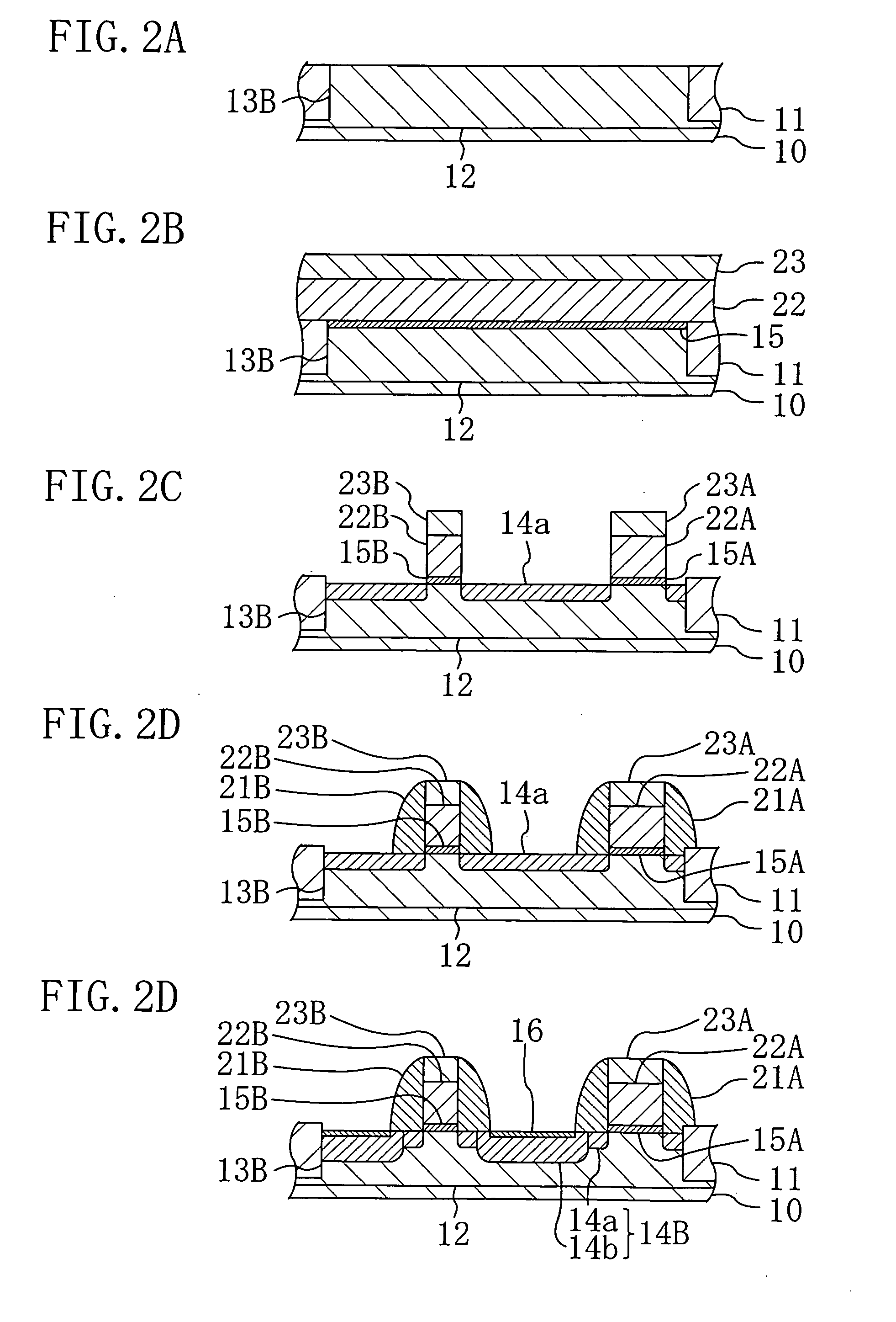
[0045] A first embodiment of the present invention will be described with reference to the drawings. FIGS. 1A and 1B illustrate a semiconductor device according to the first embodiment of the present invention. FIG. 1A illustrates a plan structure of the semiconductor device, and FIG. 1B illustrates a cross-sectional structure thereof.
[0046]FIG. 1A illustrates a first transistor 51A formed on a first active region 13A of a semiconductor substrate 10 surrounded by an isolation region 11 thereof and a second transistor 51B formed on a second active region 13B thereof. The first transistor 51A includes a fully silicided first gate electrode 17A and source/drain regions 14A formed in the first active region 13A. The second transistor 51B includes a fully silicided second gate electrode 17B and source/drain regions 14B formed in the second active region 13B. The first and second transistors 51A and 51B are both P-type MIS transistors.
[0047] As illustrated in FIG. 1B, the second transistor 51B includes a second gate insulating film 15B formed on the second active region 13B of the semiconductor substrate 10 surrounded by the isolation region 11 thereof, a second gate electrode 17B formed on the second gate insulating film 15B, second sidewalls 21B formed on both sides of the second gate electrode 17B, and source/drain regions 14B formed in regions of the second active region 13B located to both sides of the second gate electrode 17B and serving as P-type impurity diffusion layers.
[0048] The source/drain regions 14B is composed of shallow source/drain diffusion layers (extension regions or lightly-doped drain (LDD) regions) 14a formed in regions of the semiconductor substrate 10 located to both sides of the gate electrode 17B and deep source/drain diffusion layers 14b formed in regions thereof located to the outer sides of the second sidewalls 21B. Silicide layers 16 are formed on the top surfaces of the deep source/drain diffusion layers 14b.
[0049] The following layers are also formed on the second active region 13B: a first gate insulating film 15A made of the same insulating film as the second gate insulating film 15B; a fully silicided first interconnect 18A formed on the first gate insulating film 15A; and first sidewalls 21A formed on both sides of the first interconnect 18A. The first interconnect 18A has a projection part 20A projecting beyond the first sidewalls 21A and covering parts of the entire surfaces of the first sidewalls 21A and is formed continuously with the first gate electrode 17A of the first transistor 51A as illustrated in FIG. 1A. The first gate electrode 17A and the first interconnect 18A form a fully silicided first gate interconnect 19A.
[0050] As illustrated in FIG. 1A, the second gate electrode 17B is formed continuously with a fully silicided second interconnect 18B. The second gate electrode 17B and the second interconnect 18B form a fully silicided second gate interconnect 19B. The second interconnect 18B extends through the isolation region 11 toward the first active region 13A and is connected through associated one of shared contact plugs 24 to associated one of the source/drain regions 14A. The second interconnect 18B is formed, at its region on which the associated shared contact plug 24 is formed, with a projection part 20B. The second interconnect 18B formed with the projection part 20B has the same structure as the first interconnect 18A formed with the projection part 20A illustrated in FIG. 1B.
[0051] A film 34 for protecting underlayers (hereinafter, referred to as “underlayer protecting film 34”) which is formed of a silicon nitride film is formed on the semiconductor substrate 10 to cover the second gate electrode 17B, the first interconnect 18A, the first and second sidewalls 21A and 21B, and other films. An interlayer dielectric 35 made of a silicon oxide film is formed to cover the underlayer protecting film 34.
[0052] As illustrated in FIG. 1B, one of the shared contact plugs 24 is formed to cover associated one of the deep source/drain diffusion layers 14b formed in parts of the second active region 13B located to both sides of the second gate electrode 17B and part of the first interconnect 18A and pass through the interlayer dielectric 35 and the underlayer protecting film 34. One of contact plugs 25 is formed on the other one of the deep source/drain diffusion layers 14b to pass through the interlayer dielectric 35 and the underlayer protecting film 34. The contact plug 25 and the shared contact plug 24 are formed by filling contact holes with a conductive material, such as tungsten, and connected through the silicide layers 16 to the deep source/drain diffusion layers 14b.
[0053] In the semiconductor device of this embodiment, the first interconnect 18A is formed, at its part connected to associated one of the shared contact plugs 24, with a projection part 20A projecting beyond the first sidewalls 21A. The projection part 20A is wider than the other part of the first interconnect 18A. This increases the contact area between the first gate interconnect 19A and the associated shared contact plug 24. This can reduce the contact resistance between the first gate electrode 17A and the associated shared contact plug 24.
[0054] Furthermore, since the projection part 20A covers parts of the entire surfaces of the first sidewalls 21A, it functions as an etching mask in formation of contact holes passing through the interlayer dielectric 35 and the underlayer protecting film 34. This can restrain the first sidewalls 21A from being etched. In this manner, when a contact hole for formation of a shared contact plug is formed, one of the shallow source/drain diffusion layers 14a can be prevented from being exposed at the bottom of the formed contact hole. This can suppress a reduction in the junction breakdown voltage of a transistor and an increase in the junction leakage current due to shorting between the shared contact plug 24 and associated one of the shallow source/drain diffusion layers 14a.
[0055] Likewise, a second interconnect 18B is formed, at its part connected to associated one of shared contact plugs 24, with a projection part 20B projecting beyond second sidewalls 21B. The projection part 20B covers parts of the entire surfaces of the second sidewalls 21B. This reduces the contact resistance between the second gate electrode 17B and the associated shared contact plug 24.
[0056] A fabrication method for a semiconductor device according to this embodiment will be described hereinafter with reference to the drawings. FIGS. 2A through 4C are cross-sectional views illustrating process steps in the fabrication method for a semiconductor device according to the first embodiment step by step. FIGS. 2A through 4C illustrate cross sections taken along the line Ib-Ib in FIG. 1A.
[0057] First, as illustrated in FIG. 2A, an isolation region 11 for electrically isolating elements from one another is formed in a semiconductor substrate 10, for example, by shallow trench isolation (STI). In this way, a second active region 13B is formed in the semiconductor substrate 10 so as to be surrounded by the isolation region 11. Subsequently, boron ions are implanted, as a P-type impurity, into the semiconductor substrate 10, thereby forming a P-type well 12.
[0058] Next, as illustrated in FIG. 2B, a 2-nm-thick gate insulating film 15 of silicon oxide is formed on the second active region 13B by dry oxidation, wet oxidation, oxidation using radical oxygen, or any other method. Subsequently, an 80-nm-thick polysilicon film 22 that will be partially formed into gate electrodes is deposited, for example, by chemical vapor deposition (CVD), to entirely cover the semiconductor substrate 10. Thereafter, in the subsequent process step, a 60-nm-thick silicon oxide film 23 that will be partially formed into a protective film for the polysilicon film 22 is formed on the polysilicon film 22, for example, by CVD. In this case, the silicon oxide film 23 is thinner than the polysilicon film 22.
[0059] Next, as illustrated in FIG. 2C, a first protective film 23A and a second protective film 23B are formed by patterning the silicon oxide film 23 into the shape of a gate interconnect (the shape in which a gate electrode and an interconnect are continuously formed) using photolithography and dry etching.
[0060] Subsequently, the polysilicon film 22 and the gate insulating film 15 are subjected to dry etching using the patterned first and second protective films 23A and 23B as masks. In this way, the following films are formed: a first film 22A for formation of a gate interconnect (hereinafter, referred to as “first gate interconnect formation film 22A”); a first gate insulating film 15A; a second film 22B for formation of a gate interconnect (hereinafter, referred to as “second gate interconnect formation film 22B”); and a second gate insulating film 15B.
[0061] Subsequently, boron ions are implanted, as a P-type impurity, into the second active region 13B using the first gate interconnect formation film 22A and the second gate interconnect formation film 22B as masks, thereby forming P-type shallow source/drain diffusion layers 14a.
[0062] An etching gas having fluorocarbon as the main ingredient need be used for etching of the silicon oxide film 23. An etching gas having chlorine or bromine as the main ingredient need be used for etching of the polysilicon film 22.
[0063] Next, as illustrated in FIG. 2D, for example, a 50-nm-thick silicon nitride film is deposited, for example, by CVD to entirely cover the semiconductor substrate 10, and then the deposited silicon nitride film is subjected to anisotropic etching. In this way, the silicon nitride film is partially removed to leave its parts formed on both sides of a combination of the first gate interconnect formation film 22A and the first protective film 23A and both sides of a combination of the second gate interconnect formation film 22B and the second protective film 23B. In this way, first sidewalls 21A are formed to continuously cover both sides of the combination of the first gate interconnect formation film 22A and the first protective film 23A, and second sidewalls 21B are formed to continuously cover both sides of the combination of the second gate interconnect formation film 22B and the second protective film 23B.
[0064] Next, as illustrated in FIG. 2E, boron serving as a P-type impurity is introduced into the second active region 13B by ion implantation using the first sidewalls 21A and the second sidewalls 21B as masks. In this way, P-type deep source/drain diffusion layers 14b are formed in regions of the second active region 13B located to both sides of the second gate interconnect formation film 22B (located further from the second gate interconnect formation film 22B than the second sidewalls 21B). In this manner, the shallow source/drain diffusion layers 14a and the deep source/drain diffusion layers 14b form source/drain regions 14B.
[0065] Subsequently, natural oxide films formed in the top surfaces of the deep source/drain diffusion layers 14b are removed, and then a 10-nm-thick nickel film (not shown) is deposited on the semiconductor substrate 10 by sputtering. Thereafter, the semiconductor substrate 10 is subjected to the first rapid thermal annealing (RTA) in a nitrogen atmosphere, for example, at a temperature of 320° C., thereby causing a reaction between silicon forming the semiconductor substrate 10 and the nickel film.
[0066] Next, the unreacted part of the nickel film is removed using a mixed acid of hydrochloric acid and a hydrogen peroxide solution, and then the semiconductor substrate 10 is subjected to the second RTA at a higher temperature than that in the first RTA (for example, 550° C.). In this way, low-resistance silicide layers 16 are formed on the respective top surfaces of the deep source/drain diffusion layers 14b.
[0067] Next, as illustrated in FIG. 3A, a third protective film 32 that is made of a silicon oxide film and will be used as a mask for full silicidation of the first and second gate interconnect formation films 22A and 22B is formed to entirely cover the semiconductor substrate 10. Thereafter, the top surface of the third protective film 32 is planarized by CMP and polished until the respective top surfaces of the first and second protective films 23A and 23B are exposed.
[0068] Next, as illustrated in FIG. 3B, the first and second protective films 23A and 23B and an upper portion of the third protective film 32 are etched away by dry etching or wet etching with high selectivity of silicon oxide to silicon nitride and polysilicon until the respective top surfaces of the first and second gate interconnect formation films 22A and 22B are exposed. In order to selectively etch the silicon oxide film, for dry etching, the silicon oxide film need be subjected to reactive ion etching, for example, under the following conditions: Octafluorocyclopentene (C5F8), oxygen (O2) and argon (Ar) are supplied to a reaction chamber with a pressure of 6.7 Pa at flow rates of 15 ml/min (normal conditions), 18 ml/min (normal conditions) and 950 ml/min (normal conditions), respectively, using a radio frequency (RF) output power of 1800 W for plasma generation and a bias power of 1500 W; and the substrate temperature is 0° C.
[0069] Next, as illustrated in FIG. 3C, a resist mask 41 is formed to cover part of the first gate interconnect formation film 22A that will be connected to associated one of shared contact plugs 24 in a later process step. In this process step, the resist mask 41 is formed on a region of the first interconnect formation film 22A that will be formed with a projection part 20A in a later process step. Although not shown, another resist mask is formed also on a region of the second gate interconnect formation film 22B that will be formed with a projection part 20B so as to be prevented from being etched. Subsequently, part of the first gate interconnect formation film 22A that is not covered with the resist mask 41 and part of the second gate interconnect formation film 22B that is not covered with the resist mask are etched by dry etching to each have a thickness of 40 nm.
[0070] Next, as illustrated in FIG. 3D, the resist mask 41 is removed, and then a 100-nm-thick metal film 33 of nickel is deposited on the third protective film 32 by sputtering. Subsequently, the semiconductor substrate 10 is subjected to RTA in a nitrogen atmosphere at a temperature of 400° C. This causes reactions between the first gate interconnect formation film 22A and the metal film 33 and between the second gate interconnect formation film 22B and the metal film 33, resulting in the fully silicided first and second gate interconnect formation films 22A and 22B. The metal film 33 is 1.1 times or more as thick as a region of the first gate interconnect formation film 22A that will be formed with a projection part 20A. This makes it possible to filly silicide the first and second gate interconnect formation films 22A and 22B with reliability.
[0071] Next, as illustrated in FIG. 3E, unreacted part of the metal film 33 is removed. In this way, a fully silicided first gate interconnect 19A is formed of a first interconnect 18A having a projection part 20A that projects beyond the first sidewalls 21A and a first gate electrode 17A (see FIG. 1A) that does not project beyond the first sidewalls 21 (see FIG. 1A). Simultaneously, a fully silicided second gate interconnect 19B is formed of a second interconnect 18B (see FIG. 1A) having a projection part 20B (see FIG. 1A) that projects beyond the second sidewalls 21B and a second gate electrode 17B that does not project beyond the second sidewalls 21B (see FIG. 1A).
[0072] Next, as illustrated in FIG. 4A, the third protective film 32 is removed by dry etching or wet etching. Thereafter, a 50-nm-thick underlayer protecting film 34 made of a silicon nitride film is deposited, for example, by CVD to entirely cover the semiconductor substrate 10.
[0073] Next, as illustrated in FIG. 4B, an interlayer dielectric 35 made of a silicon oxide film is formed, for example, by CVD to cover the underlayer protecting film 34, and then the top surface of the interlayer dielectric 35 is planarized by CMP. Thereafter, a resist mask (not shown) is formed on the interlayer dielectric 35, and then the interlayer dielectric 35 and the underlayer protecting film 34 are subjected to dry etching using the resist mask. In this way, a first contact hole 35a is formed to expose part of associated one of the silicide layers 16 formed in the deep source/drain diffusion layers 14b, part of associated one of the first sidewalls 21A, and part of the projection part 20A of the first interconnect 18A. Simultaneously, a second contact hole 35b is formed to expose part of the other one of the silicide layers 16.
[0074] Next, as illustrated in FIG. 4C, the resist mask is removed, and then titanium (Ti) and titanium nitride (TiN) forming a barrier metal layer are deposited on the semiconductor substrate 10 by CVD to have thicknesses of 10 nm and 5 nm, respectively (not shown). Thereafter, a metal film of tungsten or any other metal is deposited on the deposited barrier metal layer.
[0075] Subsequently, a portion of the metal film deposited outside the first and second contact holes 35a and 35b and located on the top surface of the interlayer dielectric 35 is removed by CMP or an etch back process. One of shared contact plugs 24 is formed so as to be connected to associated one of the silicide layers 16 formed in the deep source/drain diffusion layers 14b and the first interconnect 18A, and one of contact plugs 25 is formed so as to be connected to the other one of the silicide layers 16.
[0076] According to the method of this embodiment, a part of the first gate interconnect formation film 22A that will be formed with the projection part 20A is thicker than the other part thereof. In such a state, the first gate interconnect formation film 22A is fully silicided. In this way, a fully silicided first gate interconnect 19A can be easily formed, at its region on which associated one of the shared contact plugs 24 is formed, with a projection part 20A. In view of the above, a semiconductor device can be easily formed which has a low contact resistance between the shared contact plug 24 and the first gate electrode 17A.
[0077] The projection part 20A of the first interconnect 18A covering parts of the entire surfaces of the first sidewalls 21A serves as an etching mask for formation of the first contact hole 35a. This can restrain the first sidewalls 21A from being etched. In view of the above, a semiconductor device can be fabricated which, even with the formation of the shared contact plugs 24, prevents a reduction in the junction breakdown voltage of a transistor and an increase in the junction leakage current thereof.
[0078] In order to form the projection part 20A covering parts of the entire surfaces of the first sidewalls 21A, the first gate interconnect formation film 22A need be fully silicided under the following conditions: The thickness of a region of the first gate interconnect formation film 22A that will be formed with the projection part 20A is half or more the height of each first sidewall 21A.
[0079] In the method of this embodiment, the height of each first sidewall 21A is substantially equal to the sum of the thickness of a region of the first gate interconnect formation film 22A that will be formed with a projection part 20A and the thickness of the first protective film 23A. In this embodiment, the region of the first gate interconnect formation film 22A that will be formed with the projection part 20A has a thickness of 80 nm, and the first protective film 23A has a thickness of 60 nm. In view of the above, the first sidewall 21A has a height of 140 nm, and therefore the thickness of the region of the first gate interconnect formation film 22A that will be formed with the projection part 20A is half or more the height of the first sidewall 21A.
[0080] The metal film 33 deposited on the first gate interconnect formation film 22A to fully silicide the first gate interconnect formation film 22A has a thickness of 100 nm and is 1.1 times or more as thick as the region of the first gate interconnect formation film 22A that will be formed with the projection part 20A. In other words, nickel is higher in amount than silicon. In such a status, Ni2Si and Ni3Si are formed in silicidation of the first gate interconnect formation film 22A. The formation of Ni2Si and Ni3Si allows a part of the fully silicided first interconnect 18A formed with the projection part 20A to become approximately twice as thick as the first gate interconnect formation film 22A of polysilicon.
[0081] A region of the first gate interconnect formation film 22A on which associated one of the shared contact plugs 24 is to be formed, i.e., a region thereof that will be formed with the projection part 20A, has a thickness of 80 nm, and each first sidewall 21A has a height of 140 nm. Therefore, since the first interconnect 18A obtained by fully siliciding the first gate interconnect formation film 22A becomes approximately twice as thick as the first gate interconnect formation film 22A, it projects beyond the first sidewalls 21A. The projection part 20A of the first interconnect 18A extends also in a lateral direction and thus covers parts of the entire surfaces of the first sidewalls 21A. Likewise, the projection part 20B of the second interconnect 18B also projects beyond the second sidewalls 21B and thus covers parts of the entire surfaces of the second sidewalls 21B.
[0082] On the other hand, a region of the second gate interconnect formation film 22B on which no shared contact plug 24 is to be formed, i.e., a region thereof that will form the second gate electrode 17B, is etched to have a thickness of 40 nm. Therefore, even when the second gate interconnect formation film 22B is fully silicided, the second gate electrode 17B does not project beyond the second sidewalls 21B. Likewise, the first gate electrode 17A does not project beyond the first sidewalls 21A.
[0083] The polysilicon film 22, the silicon oxide film 23 and the metal film 33 need be appropriately changed in thickness according to change in the size of an element to be formed. An area of the entire surface of each first sidewall 21A covered with the projection part 20A can be adjusted by changing the ratio between the thickness of the polysilicon film 22 and that of the silicon oxide film 23.
[0084] Although in this embodiment two transistors are used as an example, other transistors may be formed on a semiconductor substrate. Other elements than transistors may be formed on the semiconductor substrate. An impurity diffusion layer connected through a shared contact plug to a gate electrode is not limited to one of source/drain diffusion layers and may be, for example, one of impurity diffusion layers that are components of a diode.
[0085] In this embodiment, the first gate interconnect 19A and the second gate interconnect 19B are formed of the polysilicon film 22. However, an amorphous silicon film may be used instead of the polysilicon film. Any other semiconductor material containing silicon may be used instead.
[0086] Although a nickel film is used as a material of the metal film 33 for full silicidation of gate interconnects, any other metal film, such as platinum, may be used instead. Furthermore, although nickel is used as a metal for forming silicide layers 16, a metal for silicidation, such as cobalt, titanium or tungsten, may be used instead. CVD may be used instead of sputtering to deposit the above-mentioned metal film.
[0087] Although a silicon nitride film is used for sidewalls, a layered structure of a silicon oxide film and a silicon nitride film may be used instead.
[0088] Although in this embodiment the underlayer protecting film 34 is formed to cover transistors, an underlayer protecting film 34 does not necessarily have to be formed. In this case, the interlayer dielectric 35 need be deposited on the third protective film 32 without etching the third protective film 32.
[0089] Although the underlayer protecting film 34 is deposited after etching of the third protective film 32, the underlayer protecting film 34 may be deposited before the deposition of the third protective film 32. In this case, when the top surface of the third protective film 32 is planarized and polished by CMP to expose the top ends of the first and second protective films 23A and 23B, a part of the underlayer protecting film 34 deposited above the first and second protective films 23A and 23B is also polished and removed.

Example

[0090] A second embodiment of the present invention will be described hereinafter with reference to the drawings. FIGS. 5A and 5B illustrate a semiconductor device according to the second embodiment of the present invention. FIG. 5A illustrates a plan structure of the semiconductor device, and FIG. 5B illustrates a cross-sectional structure thereof taken along the line Vb-Vb. In FIGS. 5A and 5B, the same components as those in FIGS. 1A and 1B are denoted by the same reference numerals, and thus description thereof is not given.
[0091] As illustrated in FIG. 5B, the semiconductor device of this embodiment is configured so that the height of a part of each of first sidewalls 21A formed on both sides of a part of a first interconnect 18A on which associated one of shared contact plugs 24 is formed is lower than that of a part of each of second sidewalls 21B formed on both sides of a second gate electrode 17B. Therefore, the first interconnect 18A can be easily formed, at its region on which the associated shared contact plug 24 is formed, with a projection part 20A. Furthermore, the projection part 20A can cover parts of the top surfaces of the first sidewalls 21A with reliability. The other structure of the semiconductor device is identical with that of the first embodiment.
[0092] A fabrication method for a semiconductor device according to the second embodiment of the present invention will be described hereinafter with reference to the drawings. FIGS. 6A through 7C are cross-sectional views illustrating process steps in the fabrication method for a semiconductor device according to this embodiment. The process step of etching a second gate interconnect formation film 22B to reduce the thickness of the second gate interconnect formation film 22B to less than half the height of each of second sidewalls 21B and the previous process steps are identical with the process step illustrated in FIG. 3C and the previous process steps in the first embodiment. Therefore, their description is not given.
[0093] As illustrated in FIG. 6A, a resist mask 42 is formed to cover regions of the semiconductor substrate 10 on which gate electrodes are to be formed and expose the other region thereof on which gate interconnects each having a projection part are to be formed. Subsequently, exposed parts of the first and second sidewalls 21A and 21B located on both sides of regions of first and second gate interconnect formation film 22A and 22B that will be formed with projection parts 20A and 20B, respectively, are etched using the resist mask 42. This reduces the heights of the above-mentioned exposed parts of the first and second sidewalls 21A and 21B as compared with the other parts thereof. In other words, the height of a part of each of the first and second sidewalls 21A and 21B on which associated one of shared contact plugs 24 is to be formed is made lower than that of a part of each of the first and second sidewalls 21A and 21B formed on both sides of associated one of first and second gate electrodes 17A and 17B.
[0094] Next, as illustrated in FIG. 6B, the resist mask 42 is removed, and then a 100-nm-thick metal film 33 of nickel is deposited on a third protective film 32 by sputtering. Subsequently, the semiconductor substrate 10 is subjected to RTA in a nitrogen atmosphere at a temperature of 400° C. This causes reactions between the first gate interconnect formation film 22A and the metal film 33 and between the second gate interconnect formation film 22B and the metal film 33, resulting in the fully silicided first and second gate interconnect formation films 22A and 22B.
[0095] Next, as illustrated in FIG. 6C, unreacted part of the metal film 33 is removed. In this way, a fully silicided first gate interconnect 19A (see FIG. 5A) is formed of a first interconnect 18A having a projection part 20A that projects beyond the first sidewalls 21A and a first gate electrode 17A (see FIG. 5A) that does not project beyond the first sidewalls 21. Simultaneously, a fully silicided second gate interconnect 19B (see FIG. 5A) is formed of a second interconnect 18B (see FIG. 5A) having a projection part 20B (see FIG. 5A) that projects beyond the second sidewalls 21B and a second gate electrode 17B that does not project beyond the second sidewalls 21B.
[0096] Next, as illustrated in FIG. 7A, the third protective film 32 is removed by dry etching or wet etching. Thereafter, a 50-nm-thick underlayer protecting film 34 made of a silicon nitride film is deposited, for example, by CVD to entirely cover the semiconductor substrate 10.
[0097] Next, as illustrated in FIG. 7B, an interlayer dielectric 35 made of a silicon oxide film is formed on the underlayer protecting film 34, for example, by CVD, and then the top surface of the interlayer dielectric 35 is planarized by CMP. Thereafter, a resist mask (not shown) is formed on the interlayer dielectric 35, and then the interlayer dielectric 35 and the underlayer protecting film 34 are subjected to dry etching using the resist mask. In this way, a first contact hole 35a is formed to expose part of associated one of the silicide layers 16 formed on the deep source/drain diffusion layers 14b, part of associated one of the first sidewalls 21A, and part of the projection part 20A of the first interconnect 18A. Simultaneously, a second contact hole 35b is formed to expose part of the other one of the silicide layers 16.
[0098] Next, as illustrated in FIG. 7C, the first and second contact holes 35a and 35b are filled with a conductive material, such as tungsten, as in the first embodiment. In this way, a shared contact plug 24 is formed so as to be connected to associated one of the silicide layers 16 formed on the deep source/drain diffusion layers 14b and the first interconnect 18A. Simultaneously, a contact plug 25 is formed so as to be connected to the other one of the silicide layers 16.
[0099] According to the method of this embodiment, the height of a region of each of the first sidewalls 21A formed on both sides of a part of the first interconnect 18A on which the shared contact plug 24 is formed is made lower than that of the other region thereof. Therefore, a first gate interconnect 19A can be easily formed of a first interconnect 18A having a projection part 20A and a first gate electrode 17A having no projection part. Furthermore, the second sidewalls 21B are also allowed to have the same structure. Therefore, a second gate interconnect 19B can be easily formed of a second interconnect 18B having a projection part 20B and a second gate electrode 17B having no projection part.
[0100] In view of the above, one of the first sidewalls 21A can be restrained from being etched in the formation of the first contact hole 35a for forming a shared contact plug 24. This can restrain a leakage current from being produced due to a short circuit between the shared contact plug 24 and associated one of the shallow source/drain diffusion layers 14a.
[0101] The amount to which respective regions of the first sidewalls 21A to be covered with the projection part 20A are etched need be determined based on the thickness of a region of the first gate interconnect formation film 22A that will be formed with the projection part 20A and other elements. In this case, the top surface of the region of the first gate interconnect formation film 22A that will be formed with the projection part 20A is allowed to be at a lower level than the top end of a region of each of the first sidewalls 21A covered with the projection part 20A. Therefore, it becomes easy to partially cover the surfaces of the first sidewalls 21A. The height of each of the etched first sidewalls 21A is preferably larger than the thickness of the underlayer protecting film 34.
[0102] Although in this embodiment the second gate interconnect formation film 22B and the first sidewalls 21A are etched in this order, they may be etched in the opposite order.
[0103] As described above, the present invention is useful as a semiconductor device whose gate interconnect is fully silicided and has a local interconnect structure and a method for fabricating the same.

PUM

no PUM

Description & Claims & Application Information

We can also present the details of the Description, Claims and Application information to help users get a comprehensive understanding of the technical details of the patent, such as background art, summary of invention, brief description of drawings, description of embodiments, and other original content. On the other hand, users can also determine the specific scope of protection of the technology through the list of claims; as well as understand the changes in the life cycle of the technology with the presentation of the patent timeline. Login to view more.

Similar technology patents

Silicon crystal growing device with two-way airflow

InactiveCN101713095AReduce corrosionReduce contact areaBy pulling from meltUnder a protective fluidCartridge heaterCorrosion
Owner:芜湖升阳光电科技有限公司

Ablation catheter with grooves in surface

ActiveCN103505798AReduce contact areaReduce frictional resistanceCatheterSurgical ManipulationGuiding catheter
Owner:SHANGHAI GOLDEN LEAF MED TEC

Classification and recommendation of technical efficacy words

Why Eureka
Try Eureka