

Organic thin film transistor and method of fabricating the same
Active Publication Date: 2007-05-17
SAMSUNG DISPLAY CO LTD
View PDF11 Cites 12 Cited by
- Summary
- Abstract
- Description
- Claims
- Application Information
AI Technical Summary
Benefits of technology
[0010] An aspect of the present invention provides an organic thin film transistor (OTFT) and a method of fabricating the same in which an organic layer and metal interconnections are formed to have certain linewidths and shapes such that an increase in interconnection resistances and a corresponding degradation of device characteristics are avoided.
Problems solved by technology
However, during fabrication of the OTFT, the organic semiconductor layer can be damaged by an organic solvent when the organic semiconductor layer is produced by using a photolithography process.
Thus, device characteristics of the OTFT may be adversely affected.
In addition, the inkjet printing method neither requires use of an expensive deposition chamber nor consumes a large amount of materials.
Even when surface processing is performed, however, it is still difficult to use the inkjet printing method to produce an organic layer and metal interconnections having linewidths and shapes that are substantially uniform.
As a result, interconnection resistances are increased, thereby adversely affecting device characteristics of the OTFT.
Method used
View moreImage
Smart ImageViewing Examples

Examples
experimental example
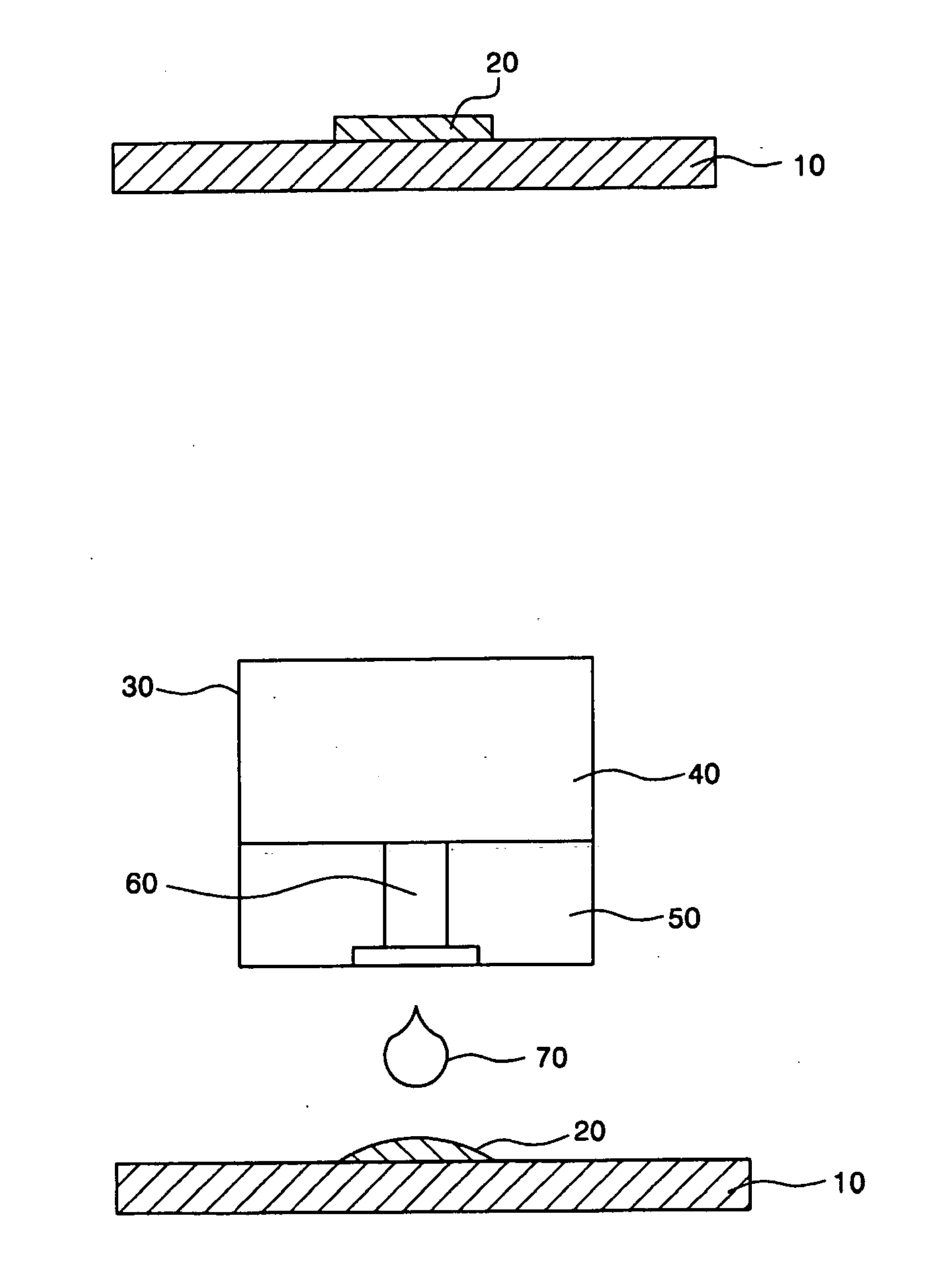
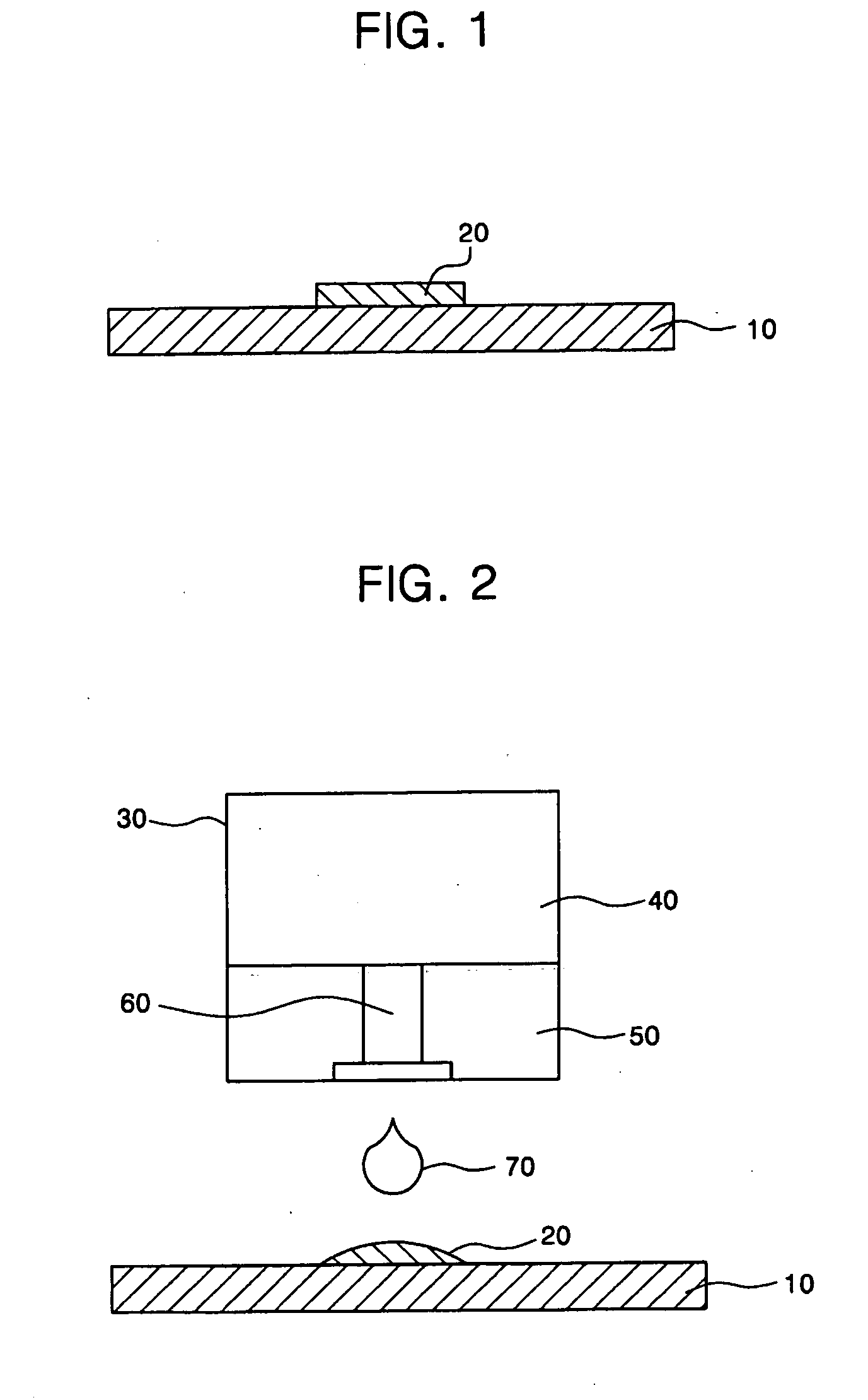
[0042] A gate electrode was formed on a substrate, and polyvinylphenol was coated on the gate electrode by use of a spin coating method such that a gate insulating layer was formed to have a thickness of 5000 Å. Thereafter, Ag ink was sprayed onto the gate insulating layer using an inkjet method, thereby forming source and drain electrodes with respective thicknesses of 1000 Å.
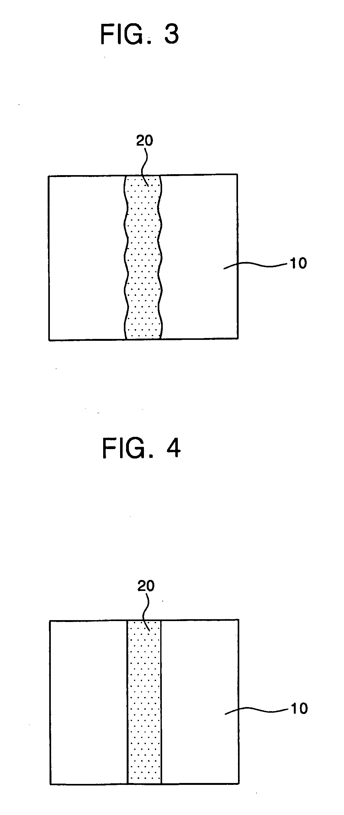
[0043] Subsequently, edge portions of the source and drain electrodes were ablated with a 248-nm KrF excimer laser. After that, a surface roughness RMS of the gate insulating layer disposed under the ablated source and drain electrodes was measured by using an atomic force microscope (AFM).
Login to View More PUM
 Abstract
An organic thin film transistor (OTFT) and a method of fabricating the same are provided in which an organic layer and metal interconnections are formed to have certain linewidths and shapes such that a degradation of device characteristics is prevented. The method includes providing a substrate, forming a gate electrode on the substrate, forming a gate insulating layer on the gate electrode, forming source and drain electrodes on the gate insulating layer, and forming a semiconductor layer on the source and drain electrodes. The gate electrode is formed by an inkjet printing method and ablated by a laser.
Description
CROSS-REFERENCE TO RELATED APPLICATION [0001] This application claims priority to and the benefit of Korean Patent Application No. 10-2005-0108043, filed on Nov. 11, 2005, in the Korean Intellectual Property Office, the entire content of which is incorporated herein by reference. BACKGROUND OF THE INVENTION [0002] 1. Field of the Invention [0003] The present invention relates to an organic thin film transistor (OTFT) and a method of fabricating the same, and more particularly, to an OTFT and a method of fabricating the same in which an organic layer and metal interconnections thereof are formed to have certain linewidths and shapes. [0004] 2. Description of the Related Art [0005] In general, a thin film transistor (TFT) includes a semiconductor layer, a gate electrode, and source and drain electrodes. In more detail, the semiconductor layer includes heavily-doped source and drain regions and a channel region interposed between the source and drain regions. The gate electrode is elec...
Claims
Login to View More Application Information
Patent Timeline
 IPC IPC(8): H01L51/40
CPCH01L51/0005H01L51/0021H01L51/0097H01L51/0545H10K71/135H10K71/60H10K10/466H10K77/111H10K71/611H10K71/621
InventorAHN, TAEKSUH, MIN-CHUL
OwnerSAMSUNG DISPLAY CO LTD