Method of manufacturing semiconductor device and semiconductor device

a manufacturing method and semiconductor technology, applied in semiconductor devices, semiconductor/solid-state device details, electrical apparatus, etc., can solve the problems of stress migration, inability to control a region having a high concentration of impurity metals to be formed at the desired place, and the interconnect resistance may increase, so as to suppress an increase in the resistance of the interconnect. , the effect of improving the stress migration lifetim

Inactive Publication Date: 2010-12-30
RENESAS ELECTRONICS CORP
View PDF7 Cites 6 Cited by
  • Summary
  • Abstract
  • Description
  • Claims
  • Application Information

AI Technical Summary

Benefits of technology

[0020]According to the invention, it is possible to improve electromigration lifetime of the interconnect and stress migration lifetime, while suppressing an increase in the interconnect resistance.

Problems solved by technology

However, there are problems in that electromigration or stress migration may occur in the interconnects in which copper is used.
In addition, stress migration occurs caused by voids generated in the interconnects.
However, according to the above method, it has been found that it is impossible to control a region having a high concentration of impurity metals to be formed at the desired place.
Moreover, in the method as disclosed in Japanese Unexamined Patent Application Publication No. 2005-050859, after the interconnect is formed, it is further required to form, heat-treat and etch the aluminum film, which results in an increase in the number of processes.
Furthermore, in the method as disclosed in Japanese Unexamined Patent Application Publication No. 2007-96241, there may be a concern that the diffusion barrier function of the copper film would not be sufficient.
However, as described above, according to the above method as described in the above documents, it has been found that it is impossible to control a region having a high concentration of impurity metals to be formed at the desired place.
For this reason, it has been found that when the surface of the plated film is polished by CMP, a large number of impurity metals are removed, and thus the sufficient amount of impurity metals does not remain in the interconnect film after CMP.
For this reason, it has not been possible to provide a region having a high concentration of the impurity metals in a desired place of the interconnect.
On the other hand, there has been a problem that annealing is not performed after growth of the plated film, the grains do not grow, and thus the interconnect resistance increases.

Method used


Image

  • Method of manufacturing semiconductor device and semiconductor device
  • Method of manufacturing semiconductor device and semiconductor device
  • Method of manufacturing semiconductor device and semiconductor device

Examples


example 1

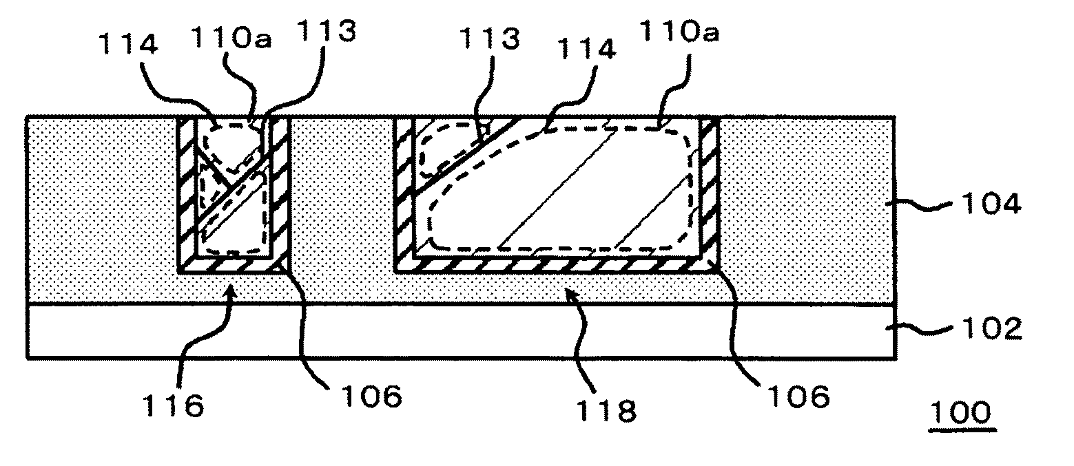
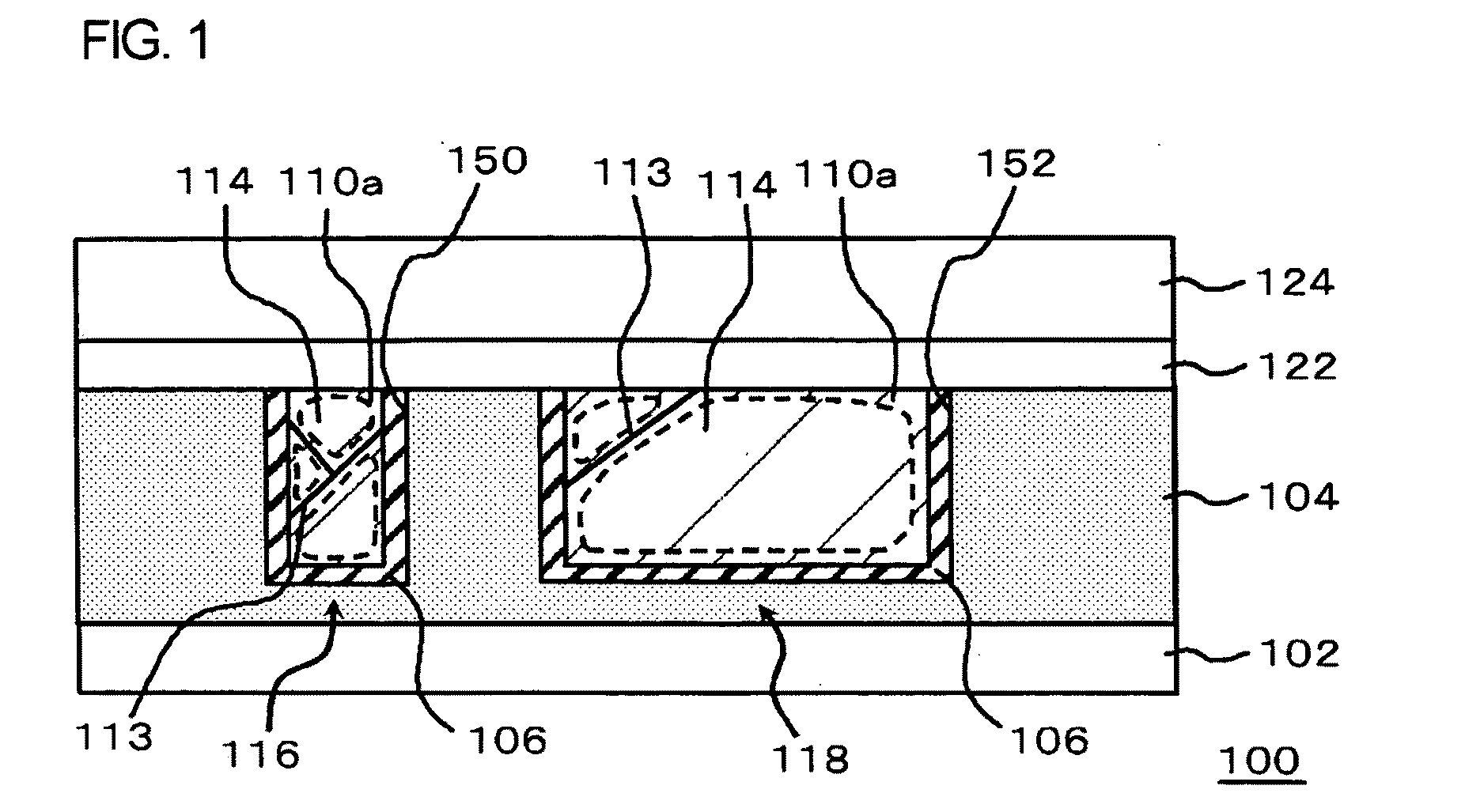
[0058]The semiconductor device was manufactured by the manufacturing procedure of the semiconductor device described with reference to FIGS. 1 to 5B. FIG. 7 is a cross-sectional view (BF-STEM image) illustrating the configuration of the narrow-width interconnect 116. Herein, the interconnect width was set to 50 nm. A stacked film (total film thickness of 7 nm) of a Ta film and a TaN film was used as the barrier metal film 106. In addition, Al was used as the impurity metal. The content of Al was set to 0.5 wt %. The film thickness of the seed alloy film 110 was set to 5 nm. The first annealing condition was set to a processing time of thirty seconds and a processing temperature of 350° C. In addition, the second annealing condition was set to a processing time of thirty minutes and a processing temperature of 350° C.

[0059]The elemental analysis was performed by the energy dispersive X-ray spectrometer (EDX), using the interconnect surface surrounded by the dashed line “1” and the ce...

example 2

[0063]Similarly to Example 1, the semiconductor device was manufactured by the manufacturing procedure of the semiconductor device described with reference to FIGS. 1 to 5B. FIG. 8 is a cross-sectional view (BF-STEM image) illustrating the configuration of the narrow-width interconnect 116. The condition was the same as Example 1. The darker shaded area in the interconnect metal film 114 of FIG. 8 is a place in which the grain boundary 113 is distributed. “3” and “4” of FIG. 8 exist in the grain boundary 113. “5” exists in the inside of the grains of the interconnect metal film 114.

[0064]The elemental analysis of the cross section of the narrow-width interconnect 116 was performed by the EDX. The elemental analysis was performed using the grain boundary indicated by “3”, the grain boundary indicated by “4”, and the inside of the grains indicated by “5” of FIG. 8, respectively, as the analysis points. The respective content of Al to all the elements in the respective analysis regions...


PUM

PropertyMeasurementUnit
temperatureaaaaaaaaaa
processing temperatureaaaaaaaaaa

Abstract

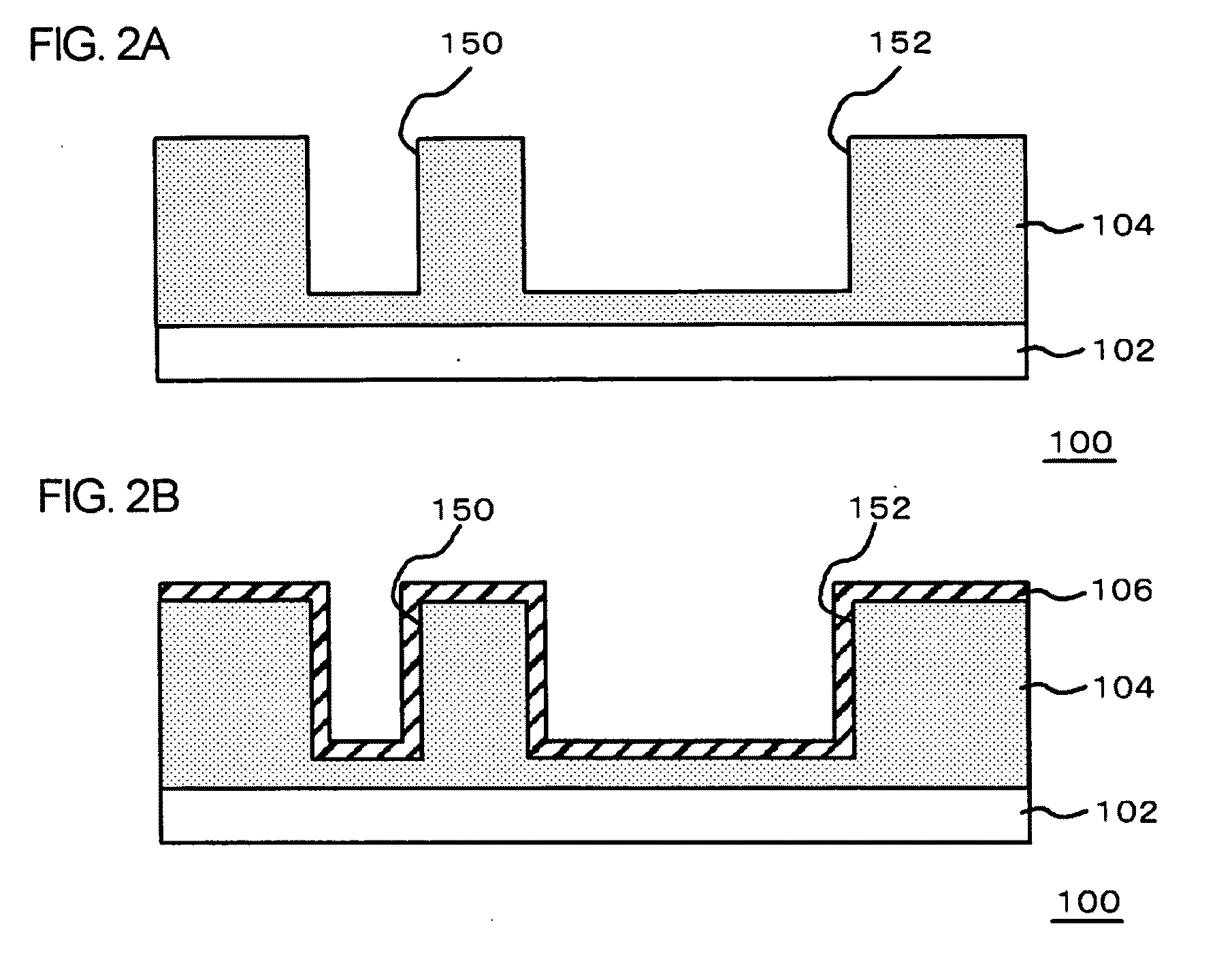
A method of manufacturing a semiconductor device includes forming a barrier metal film including a high melting point metal in a concave portion formed in an insulating film formed over a substrate; forming a seed alloy film including copper and an impurity metal different from the copper over the barrier metal film so as to fill a portion of the concave portion; forming a plated metal film containing copper as a major ingredient over the seed alloy film so as to fill the concave portion; first heat-treating the seed alloy film and the plated metal film at 200° C. or higher and for ten minutes or less; removing the plated metal film, the seed alloy film, and the barrier metal film which are exposed to the outside of the concave portion, after the first heat-treating; and second heat-treating the seed alloy film and the plated metal film.

Description

[0001]The application is based on Japanese patent application No. 2009-151129, the content of which is incorporated hereinto by reference.BACKGROUND[0002]1. Technical Field[0003]The present invention relates to a method of manufacturing a semiconductor device and the semiconductor device.[0004]2. Related Art[0005]From the request for high integration of semiconductor devices in recent years, copper having a low resistance has been widely used as a material for interconnects, plugs, pads and the like. However, there are problems in that electromigration or stress migration may occur in the interconnects in which copper is used. Although the copper film that constitutes the copper interconnects is typically formed by a plating method. When the copper interconnects is formed by a plating method, the copper film is formed so that a large number of copper particles having a polycrystalline structure are collected. When voltage is applied to the copper interconnects having such a structur...

Claims


Application Information

Patent Timeline
Patent Type & Authority Applications(United States)
IPC IPC(8): H01L23/532H01L21/768
CPCH01L21/7684H01L21/76873H01L21/76877H01L21/76883H01L23/5283H01L23/53233H01L2924/0002H01L23/53238H01L23/5329H01L2924/00
Inventor IGUCHI, MANABUAIZAWA, HIROKAZU
Owner RENESAS ELECTRONICS CORP
Why Eureka
Try Eureka