Amplification-type CMOS image sensor of wide dynamic range

a cmos image sensor and wide dynamic range technology, applied in the field of solid-state image sensing devices, can solve the problems of reducing image quality, affecting image quality, and affecting image quality,

Active Publication Date: 2007-05-03
KK TOSHIBA
View PDF12 Cites 51 Cited by
  • Summary
  • Abstract
  • Description
  • Claims
  • Application Information

AI Technical Summary

Benefits of technology

[0020]FIG. 13 is a photoelectric conversion characteristic diagram for illustrating the effect of the solid-state image sensing device according to the fourth embodiment of this invention.

Problems solved by technology

The former method is applied to incomplete transfer type photodiodes, but in this case, there is a possibility that residual images and white defects will occur and it is difficult to enhance the image quality.
However, since the dynamic range is widened by use of a detecting section, unevenness of dark-time and KTC noises due to a leak current in the detecting section are generated and there occurs a possibility that the image quality will be degraded due to a factor different from that of the former method.
In addition, since signals of long exposure time and short exposure time are added and output in each of the above methods, it is difficult to separate the signals of long exposure time and short exposure time from each other.

Method used


Image

  • Amplification-type CMOS image sensor of wide dynamic range
  • Amplification-type CMOS image sensor of wide dynamic range
  • Amplification-type CMOS image sensor of wide dynamic range

Examples


first embodiment

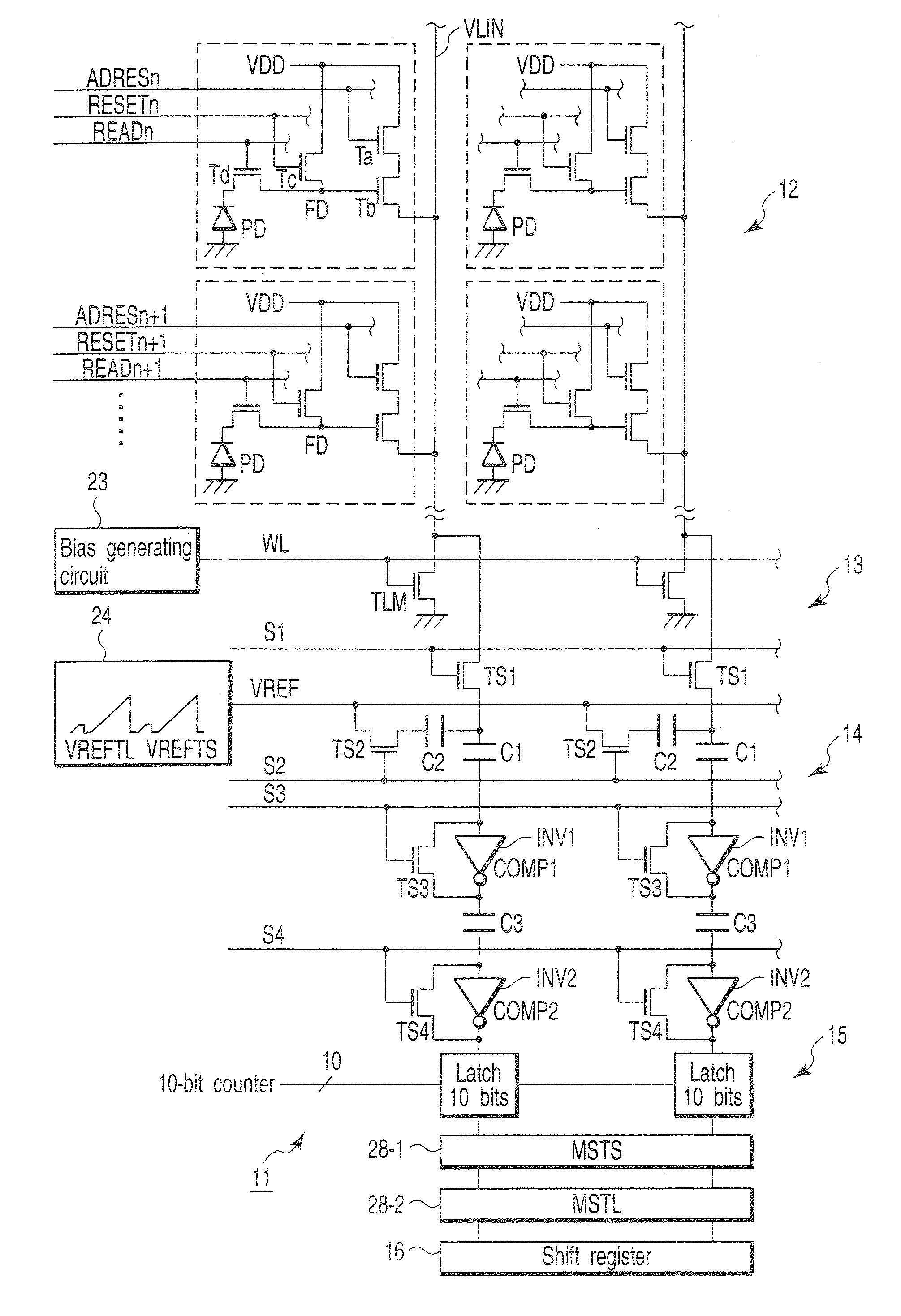
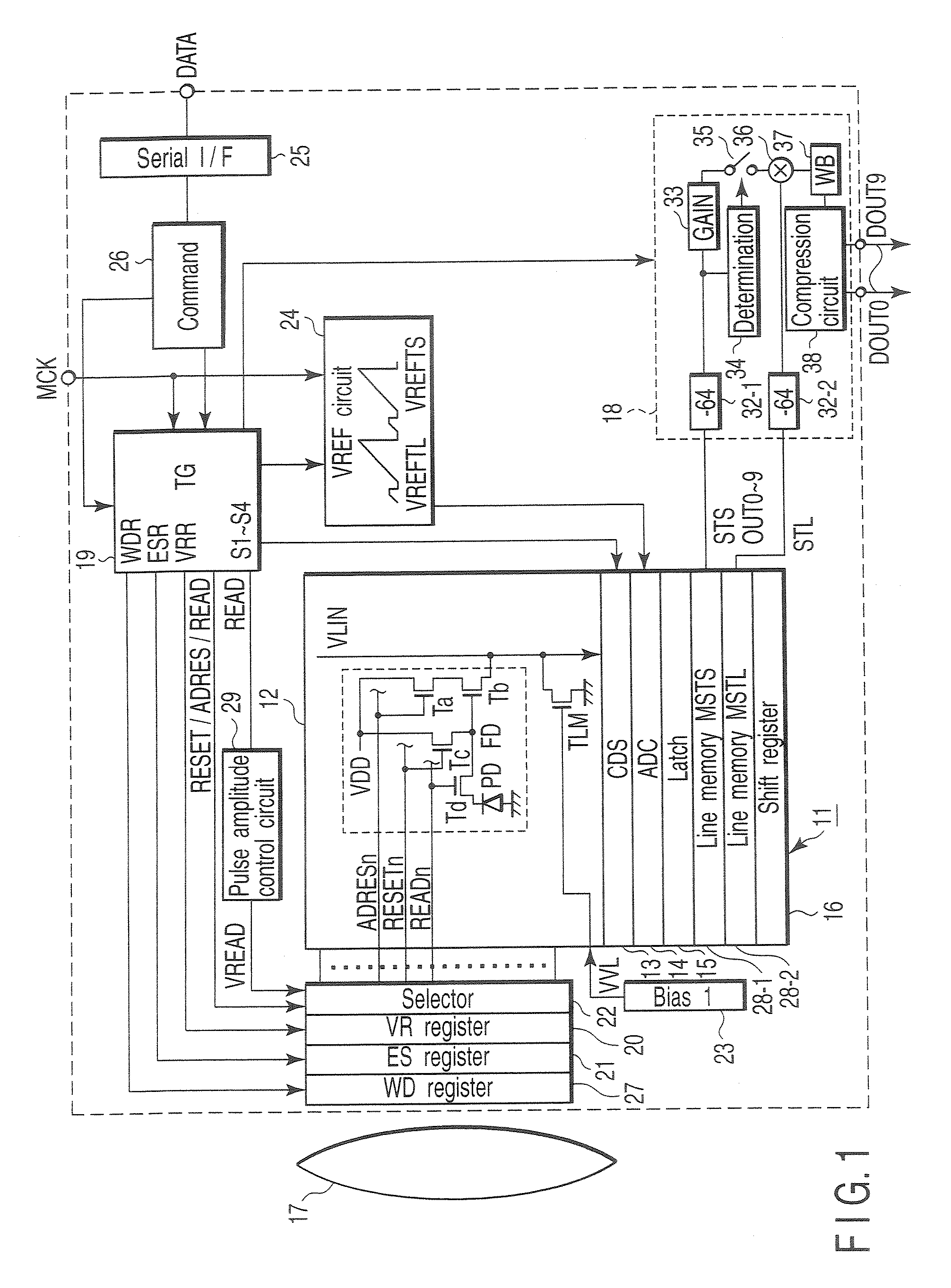
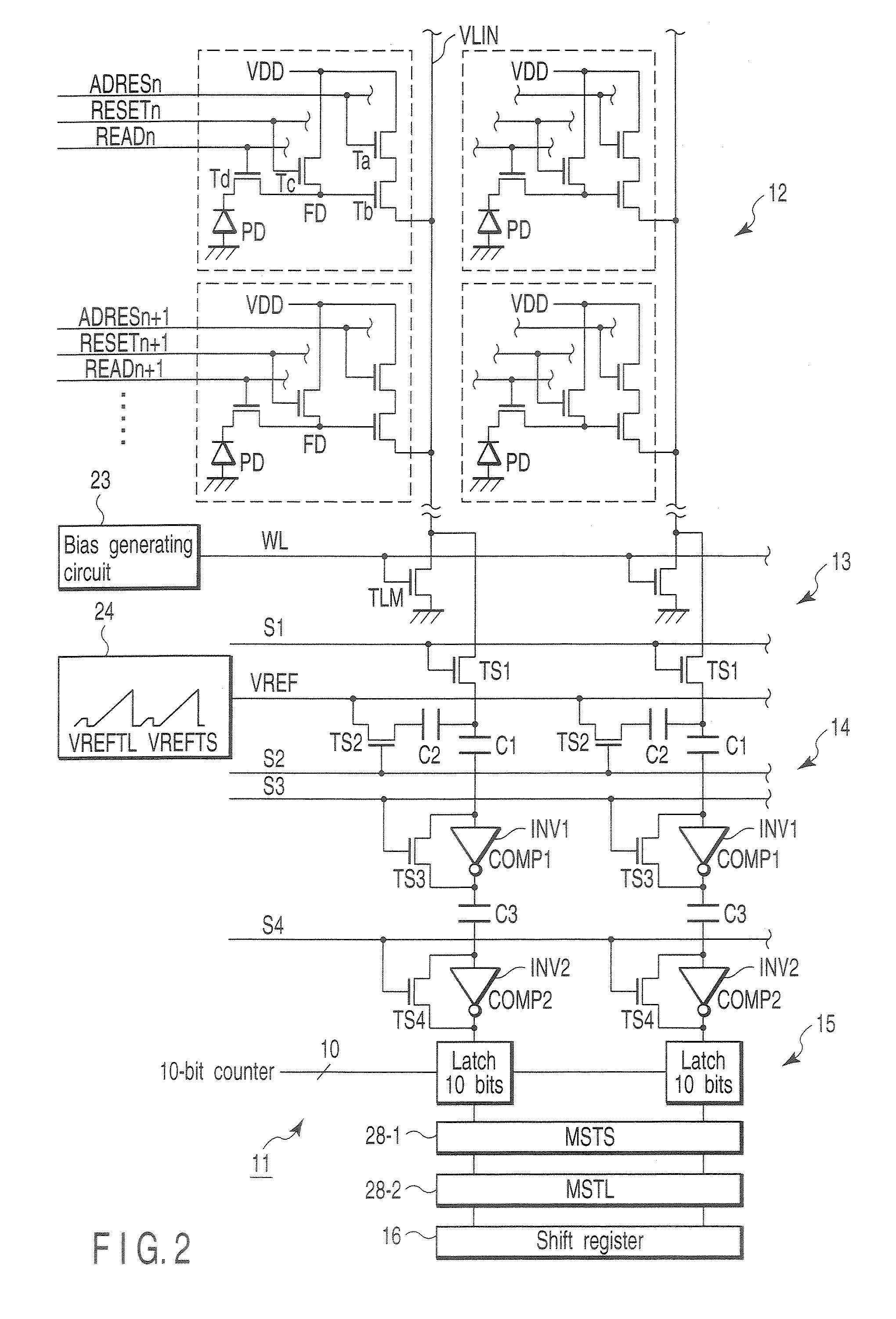
[0021]FIG. 1 is a block diagram showing the schematic configuration of an amplification-type CMOS image sensor, for illustrating a solid-state image sensing device according to a first embodiment of this invention. In a sensor core section 11, a pixel section 12, column type noise canceling circuit (CDS) 13, column type analog-digital converter (ADC) 14, latch circuit 15, two line memories (MSTS, MSTL) 28-1, 28-2, horizontal register 16 and the like are arranged.

[0022] Light is incident on the pixel section 12 via a lens 17 and charges corresponding to an incident light amount are generated by photoelectrical conversion. In the pixel section 12, cells (pixels) are arranged in a two-dimensional form of rows and columns on a semiconductor substrate. Each cell is configured by four transistors (Ta, Tb, Tc, Td) and a photodiode (PD) and pulse signals ADRESn, RESETn and READn are supplied to each cell. In the lower portion of the pixel section 12, load transistors TLM of a source follow...

second embodiment

[0042]FIG. 4 shows the photoelectric conversion characteristic of the CMOS image sensor shown in FIGS. 1 and 2. A signal STL is saturated at an SVm level. If the signal STL is saturated, a signal STS is output. When the level of the signal STS is increased, a Knee point is generated and the inclination thereof is suppressed by the accumulation time ratio TS / TL. Therefore, if the signal processing operation is performed by use of a WDM circuit 18 with the configuration as shown in FIG. 1, a small-signal portion of the signal STS is greatly amplified and added and, as a result, the level of an added output signal SF is lifted in a range higher than SVm. The inclination of a portion after the Knee point is set to the same as that of the signal STL, but the signal is lifted by an amount corresponding to the offset. However, when the accumulation time ratio TS / TL is sufficiently low, the Knee point is set at substantially the same level as ΦVm, and therefore, the signal can be practicall...

third embodiment

[0052] In the second embodiment, the photodiode PD section performs an incomplete transfer operation in a portion near the Knee point of the signal STS as more precisely shown in FIG. 7. Therefore, a state in which a residual image occurs and the signal becomes difficult to be read is set and the characteristic is smoothly curved. When signal charges of an amount sufficiently larger than that of the Knee point are present in the photodiode PD section, the signal charges themselves act as bias charges to suppress occurrence of the residual image, and therefore, no residual image occurs and the characteristic linearly varies. If the Knee point having the smooth characteristic curve is subjected to the WDM process, the linearity of the synthesized signal SF is deteriorated in a portion near the Knee point. In the experiment, a deterioration of 5% at maximum occurs with respect to the ideal characteristic.

[0053]FIG. 8 is a block diagram showing the schematic configuration of an amplifi...


PUM


Abstract

A solid-state image sensor which includes a pixel section, AD converter, line memory, controller and synthesizer is disclosed. The line memory stores a digital signal output from the AD converter. The controller controls the pixel section and AD converter to subject analog signals of different exposure times to an AD converting process by use of the AD converter and transfer the thus AD-converted signals to the line memory in an accumulation period of charges of one frame. The synthesizer is supplied with digital signals of different exposure times from the line memory, compare a fist signal obtained by adding signals of short and long exposure times with a second signal obtained by amplifying the signal of short exposure time by the ratio of the signal of short exposure time to the signal of long exposure time, select a larger one of the compared signals and output the selected signal.

Description

CROSS-REFERENCE TO RELATED APPLICATIONS [0001] This application is based upon and claims the benefit of priority from prior Japanese Patent Application No. 2005-315409, filed Oct. 28, 2005, the entire contents of which are incorporated herein by reference. BACKGROUND OF THE INVENTION [0002] 1. Field of the Invention [0003] This invention relates to a solid-state image sensing device which can be applied, for example, to an amplification-type CMOS image sensor used in a mobile telephone with an image sensor, digital camera, video camera or the like. [0004] 2. Description of the Related Art [0005] Conventionally, methods for widening the dynamic range of a CMOS image sensor are proposed in Jpn. Pat. Appln. KOKAI Publication No. 2001-189893 and Jpn. Pat. Appln. KOKAI Publication No. 2000-23044, for example. The former method is applied to incomplete transfer type photodiodes, but in this case, there is a possibility that residual images and white defects will occur and it is difficult ...

Claims


Application Information

Patent Timeline
Patent Type & Authority Applications(United States)
IPC IPC(8): H04N5/335H04N5/353H04N5/355H04N5/374H04N5/376H04N5/378
CPCH04N5/235H04N5/2355H04N5/335H04N23/70H04N23/741H04N25/00H04N25/583H04N25/76H04N25/75
Inventor EGAWA, YOSHITAKAOKAMOTO, RYUTAOHSAWA, SHINJIGOTO, HIROSHIGE
Owner KK TOSHIBA
Why Eureka
Try Eureka