Compound-eye imaging device

a technology of compound eye and imaging device, which is applied in the field of compound eye imaging device, can solve the problems of increasing the integration density reducing the size of the optical lens, and difficulty in manufacturing, and achieves the effect of reducing the thickness

Inactive Publication Date: 2007-05-03
FUNAI ELECTRIC CO LTD
View PDF4 Cites 32 Cited by
  • Summary
  • Abstract
  • Description
  • Claims
  • Application Information

AI Technical Summary

Benefits of technology

[0011] An object of the present invention is to provide a compound-eye imaging device which can be reduced in its thickness without either causing difficulties in manufacturing or causing a problem that it takes a long time to reconstruct an image.
[0014] The compound-eye imaging device according to the present invention makes it possible to reduce the focal length of each optical lens, as compared with the case of forming an optical lens array or optical lenses by using an ordinary glass material, thereby reducing the thickness of the compound-eye imaging device without either causing a difficulty in manufacturing or causing a problem of taking a long time to reconstruct an image.

Problems solved by technology

However, there are problems in reducing the size of each optical lens, and increasing the integration density of the optical lenses.
That is, first, this causes a difficulty in manufacturing.
Second, the increase in the number of optical lenses causes the number of single-eye images formed on the photodetector array to increase, so that it takes a long time to reconstruct the single-eye images into one image by using parallax information between the single-eye images.

Method used


Image

  • Compound-eye imaging device
  • Compound-eye imaging device
  • Compound-eye imaging device

Examples


Embodiment Construction

[0028] Embodiments of the present invention, as best mode for carrying out the invention, will be described hereinafter with reference to the drawings. The present invention relates to a compound-eye imaging device. It is to be understood that the embodiments herein are not intended as limiting, or encompassing the entire scope of, the invention. Note that like parts are designated by like reference numerals or characters throughout the drawings.

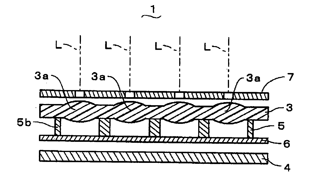
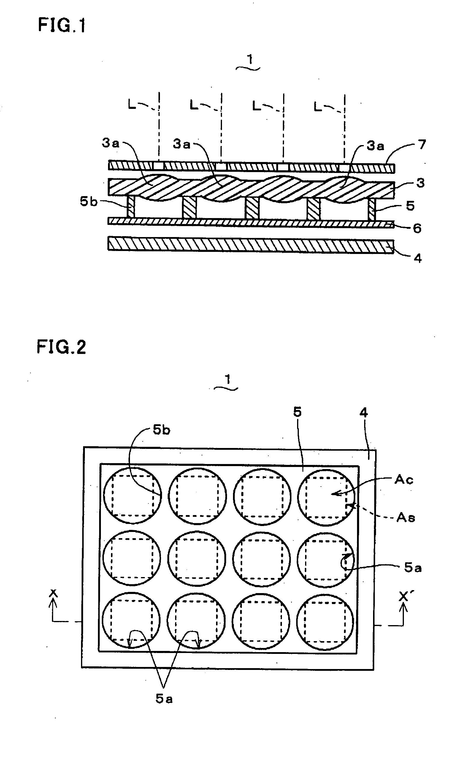
[0029] A compound-eye imaging device 1 according to a first embodiment of the present invention will be described with reference to FIG. 1, FIG. 2, FIG. 3, FIG. 6A and FIG. 6B. FIG. 1 is a schematic side cross-sectional view of the compound-eye imaging device 1 according to the first embodiment of the present invention along line X-X′ of FIG. 2, while FIG. 2 is a schematic plan view of the compound-eye imaging device 1, showing a light shielding block 5 and a photodetector array 4. As shown in FIG. 1 and FIG. 2, the compound-eye imaging dev...


PUM


Abstract

A compound-eye imaging device comprises: an optical lens array with integrated optical lenses; a stop member for shielding unnecessary ambient light from entering the optical lens array; a photodetector array placed at a predetermined distance from the optical lens array for imaging images formed by the optical lenses; and a light shielding block placed between the two arrays for partitioning a space between the two arrays into a matrix of spaces as seen on a plane perpendicular to the optical axis of each optical lens to prevent lights from the optical lenses from interfering each other. The optical lenses are formed of a molded glass having a refractive index distribution to increase the refractive index of each optical lens in the direction of light propagation. The focal length of each optical lens can be reduced as compared with an ordinary lens, thereby reducing the thickness of the compound-eye imaging device.

Description

BACKGROUND OF THE INVENTION [0001] 1. Field of the Invention [0002] The present invention relates to a compound-eye imaging device having an optical imaging system which is formed of multiple micro optical systems so as to reduce the focal length, enabling reducing the thickness of the compound-eye imaging device. [0003] 2. Description of the Related Art [0004] There has been developed a compound-eye imaging device as a thin camera module to be installed in a cellular phone, a personal computer, or the like. The compound-eye imaging device is mainly composed of: an optical lens array with multiple integrated optical lenses having optical axes parallel to each other; a photodetector array for imaging multiple single-eye images formed by the respective optical lenses of the optical lens array; and an image reconstructing circuit for reconstructing the multiple single-eye images, imaged by the photodetector array, into one image by using parallax information between the multiple single...

Claims


Application Information

Patent Timeline
Patent Type & Authority Applications(United States)
IPC IPC(8): G02B27/10
CPCG02B3/0031G02B3/0056G02B3/0068G02B3/0075G02B7/021
Inventor TOYODA, TAKASHINAKAO, YOSHIZUMIMASAKI, YASUO
Owner FUNAI ELECTRIC CO LTD
Why Eureka
Try Eureka