Non-volatile memory device and method of manufacturing the same

Inactive Publication Date: 2007-05-10
DONGBU ELECTRONICS CO LTD
View PDF3 Cites 0 Cited by
  • Summary
  • Abstract
  • Description
  • Claims
  • Application Information

AI Technical Summary

Benefits of technology

[0021] The present invention has been made in an effort to provide a non-volatile memory device and method of manufacturing the same having a advantage that the non-volatile memory device

Problems solved by technology

However, since a conventional method of manufacturing a non-volatile memory device has a limit for reducing a cell size while assuring

Method used


Image

  • Non-volatile memory device and method of manufacturing the same
  • Non-volatile memory device and method of manufacturing the same
  • Non-volatile memory device and method of manufacturing the same

Examples


Embodiment Construction

[0028] An exemplary embodiment of the present invention will hereinafter be described in detail with reference to the accompanying drawings.

[0029]FIG. 3A to 3G and FIG. 4A to FIG. 4G are cross-sectional views and top plan views showing a method of manufacturing a non-volatile memory device according to an exemplary embodiment of the present invention.

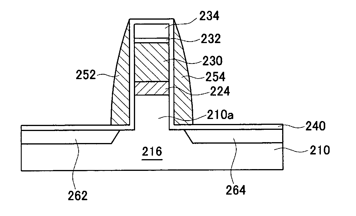
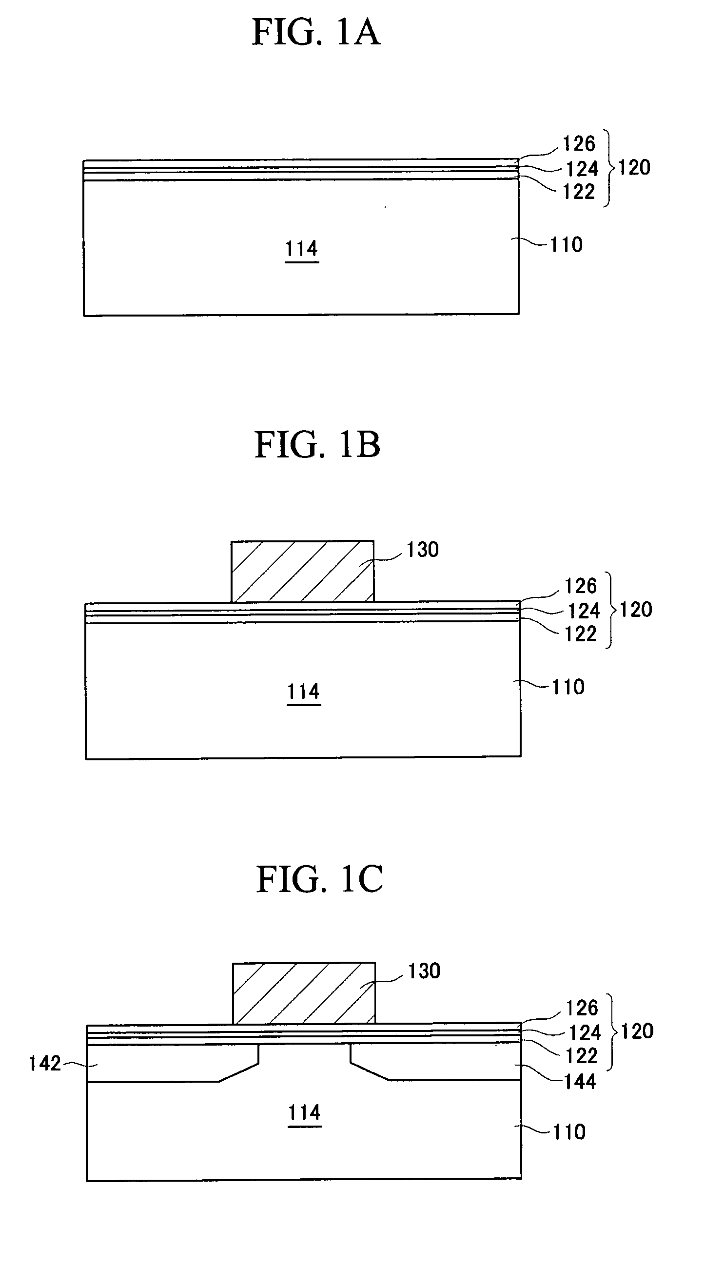
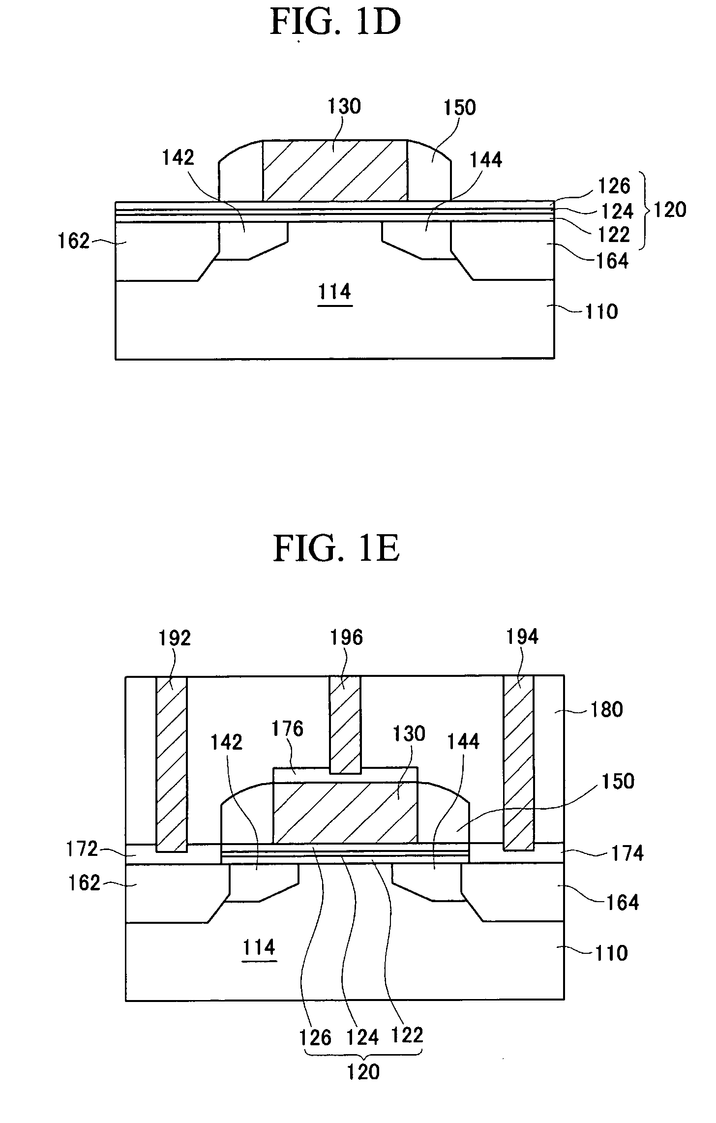
[0030] Referring to FIG. 3A and FIG. 4A, a mask pattern (not shown) composed of a pad oxide layer and a pad nitride layer is formed on a semiconductor substrate 210, and a trench (not shown) is formed by etching a portion of the substrate 210 exposed by the mask pattern.

[0031] Subsequently, an oxide layer is deposited so as to fill the trench, and an isolation layer 214 is formed by planarizing the oxide layer through a chemical mechanical polishing (CMP) process and by removing the mask pattern. Consequently, an active region 216 is defined on the semiconductor substrate 110 by forming the isolation layer 214. Thereafter, a pad oxid...


PUM


Abstract

A non-volatile memory device and a method of manufacturing the same where the non-volatile memory device is easily applicable to higher integration of a semiconductor device by reducing a cell size while assuring storage capacities required for operations of a device. The non-volatile memory device includes a semiconductor substrate in which an active region is defined by an isolation layer and a protruding portion is formed on the active region, a source region formed on the protruding portion, first and second gates formed at both sidewalls of the protruding portion and the source region, first and second drain regions formed in the active region at the outside of the first and second gates, and an insulation layer formed between the first and second gates and the protruding portion and the source region.

Description

CROSS-REFERENCE TO RELATED APPLICATION [0001] This application claims priority to and the benefit of Korean Patent Application No. 10-2005-0097009 filed in the Korean Intellectual Property Office on Oct. 14, 2005, the entire contents of which are incorporated herein by reference. BACKGROUND OF THE INVENTION [0002] (a) Field of the Invention [0003] The present invention relates to a method of manufacturing a semiconductor device. More particularly, the present invention relates to a SONOS non-volatile memory device and a method of manufacturing the same. [0004] (b) Description of the Related Art [0005] Generally, since a non-volatile memory device has several merits, such as a small cell size, fast erasing and programming operation, and long-term capacity of data storage, then a non-volatile memory device is frequently used as a signaling transistor in a personal digital assistant (PDA), a digital camera, a personal communication system (PCS), and a smart card, or as a memory device ...

Claims


Application Information

Patent Timeline
IPC IPC(8): H01L29/788
CPCH01L21/28282H01L29/42344H01L29/66833H01L29/792H01L29/7926H01L29/40117H01L21/76897
Inventor LEE, SANG-BUM
Owner DONGBU ELECTRONICS CO LTD
Why Eureka
Try Eureka