Fabrication of polymer waveguide using a mold

Inactive Publication Date: 2007-05-10
LUVANTIX CO LTD
View PDF1 Cites 20 Cited by
  • Summary
  • Abstract
  • Description
  • Claims
  • Application Information

AI Technical Summary

Benefits of technology

[0004] Accordingly, it is a primary object of the present invention to provide an effic

Problems solved by technology

These conventional methods, however, are hampered by the problem that a lip is

Method used


Image

  • Fabrication of polymer waveguide using a mold
  • Fabrication of polymer waveguide using a mold
  • Fabrication of polymer waveguide using a mold

Examples


example 1

Design of an Assembly for a Mold

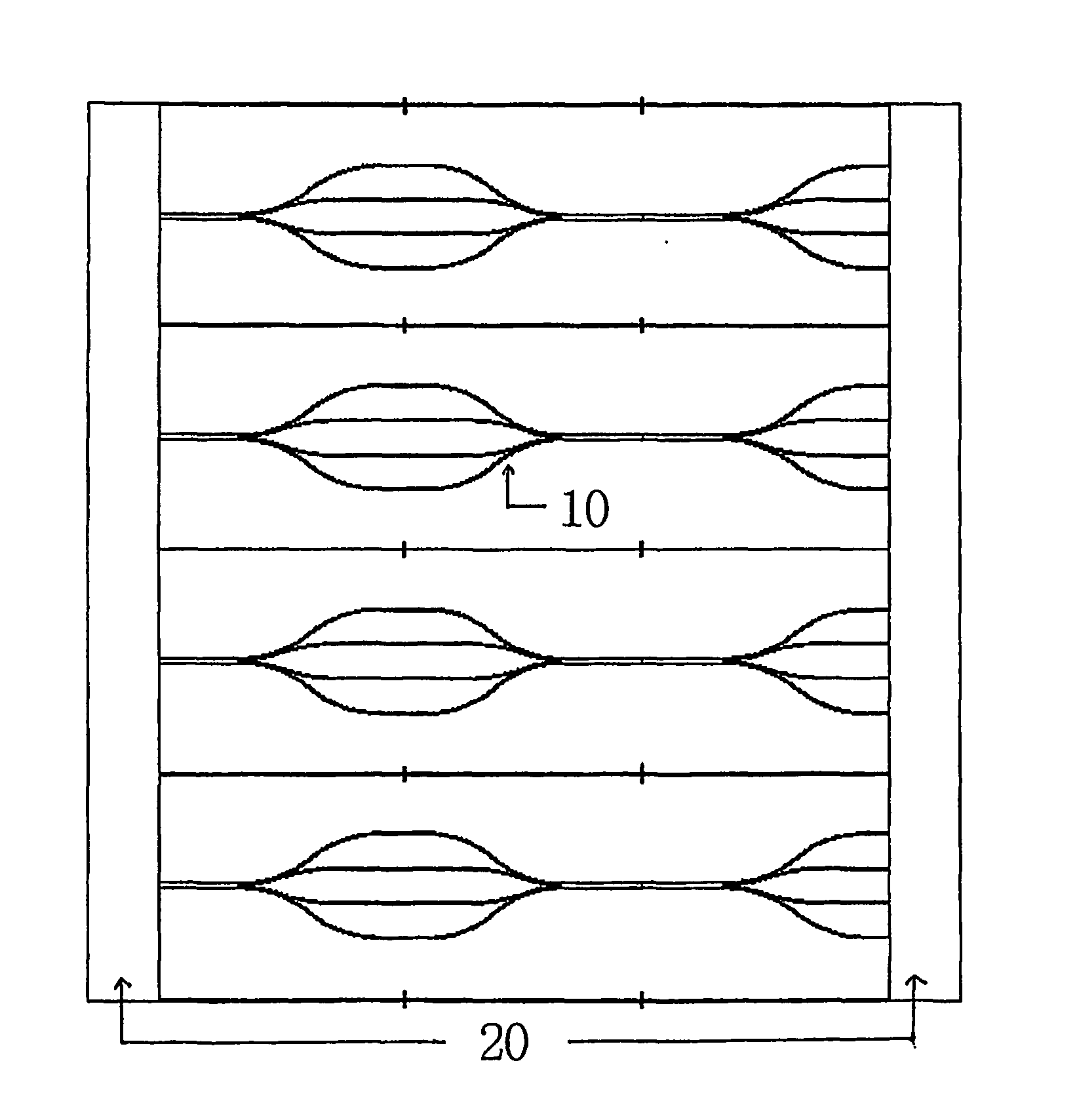
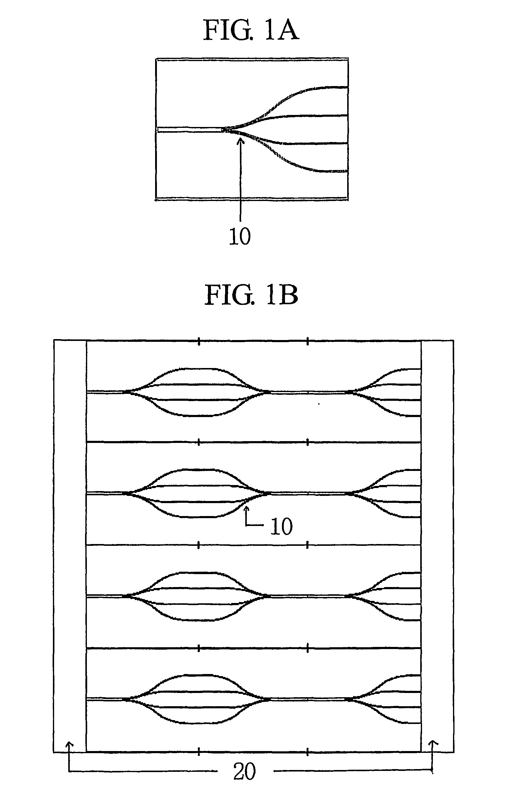
[0025] A waveguide pattern unit (10) was designed in the form of a cascade-type 1×4 multi-mode splitter unit having a width×length of 65 mm×70 mm, wherein one major channel (400 μm×200 μm (width×depth)) splits into four branch channels (200 μm×200 μm (width×depth)) as shown in FIG. 1A. Twelve of such units were arranged in a four row×three column configuration together with two rectangular band parts (20) having a width×length of 5 mm×5 mm and a depth of 200 μm such that the channels of the units in each row were interconnected with each other and also to the two bands, as shown in FIG. 1B, to obtain an assembly for a mold.

Preparation of a Mold

example 2

Preparation of a Rubber Mold—1

[0026] A photomask was prepared using the assembly obtained in Example 1. An SU-8 photoresist was coated on a silicon wafer, dried and light-exposed using a mask-aligner and the prepared photomask, and treated with a developer, to prepare an embossing photoresist master. An aluminum tape wall was installed on the circumference of the master. A polydimethylsiloxane rubber was poured thereto, kept at room temperature to remove bubbles therefrom, and cured at 50° C. for 3 hrs, to obtain a rubber mold having a recessed shape.

example 3

Preparation of a Rubber Mold—2

[0027] A photomask was prepared using the assembly obtained in Example 1. The photomask was placed on a 5 mm thick nickel metal plate and subject to LIGA, to prepare an embossing master. For enhancing the surface roughness, the master was nickel plated and polished. An aluminum tape wall was installed on the circumference of the master. A polydimethylsiloxane rubber was poured thereto, kept at room temperature to remove bubbles therefrom, and cured at 50° C. for 3 hrs, to obtain a rubber mold having a recessed shape.


PUM


Abstract

A polymer waveguide having low optical loss and no lip around a core is prepared by using a mold having a recessed shape formed by assembling at least two waveguide pattern units having predesigned channels together with two band parts such that the channels of the units are interconnected and open to the band parts, and filling the void generated by contacting the mold and a under cladding layer with a photocurable polymeric resin to form a core layer.

Description

FIELD OF THE INVENTION [0001] The present invention relates to a method for preparing a polymer waveguide comprising a core and at least one cladding layer, the waveguide having low optical loss and no lip around its core, using a mold having a recessed shape for forming the core pattern. BACKGROUND OF THE INVENTION [0002] Multi-mode optical waveguides comprising an under cladding layer, a core layer which serves as a multi-mode transport channel and an upper cladding layer are employed in short distance communication, e.g., LAN (local area network), building network, access network, optical backplane and optical interconnection. Such optical waveguides have been produced using an inexpensive polymer such as polyimides, epoxides and acrylates instead of silica. [0003] Further, various techniques have been reported by Jenoptik Mikrotechnik GmbH. in Germany, and Chou at Prinston University and Whiteside at Harvard University in United States, which produce a core layer by press-emboss...

Claims


Application Information

Patent Timeline
IPC IPC(8): G02B6/10B29D11/00G02B6/12G02B6/122G02B6/138
CPCB29D11/00663B29L2011/0075G02B6/12004G02B6/1221G02B6/138G02B6/12
Inventor KIM, MAL-SOONYUN, JUNG-WOOOH, JUNG-HYUN
Owner LUVANTIX CO LTD
Why Eureka
Try Eureka