Method and apparatus for manufacturing a semiconductor device, control program thereof and computer-readable storage medium storing the control program

Inactive Publication Date: 2007-05-10
TOKYO ELECTRON LTD
View PDF2 Cites 14 Cited by
  • Summary
  • Abstract
  • Description
  • Claims
  • Application Information

AI Technical Summary

Benefits of technology

[0016] In accordance with the present invention, it is possible to prevent a generation of roughness on a silicon

Problems solved by technology

In the above method, an addition of O2 gas increases the selectivity of the silicon nitride film against the silicon oxide film, since the O2 gas contained in the etching gas hardly contributes to the etching of the silicon oxide film.
When the selectivity of the silicon nitride film against the silicon oxide film is increased by addin

Method used


Image

  • Method and apparatus for manufacturing a semiconductor device, control program thereof and computer-readable storage medium storing the control program
  • Method and apparatus for manufacturing a semiconductor device, control program thereof and computer-readable storage medium storing the control program
  • Method and apparatus for manufacturing a semiconductor device, control program thereof and computer-readable storage medium storing the control program

Examples


Example

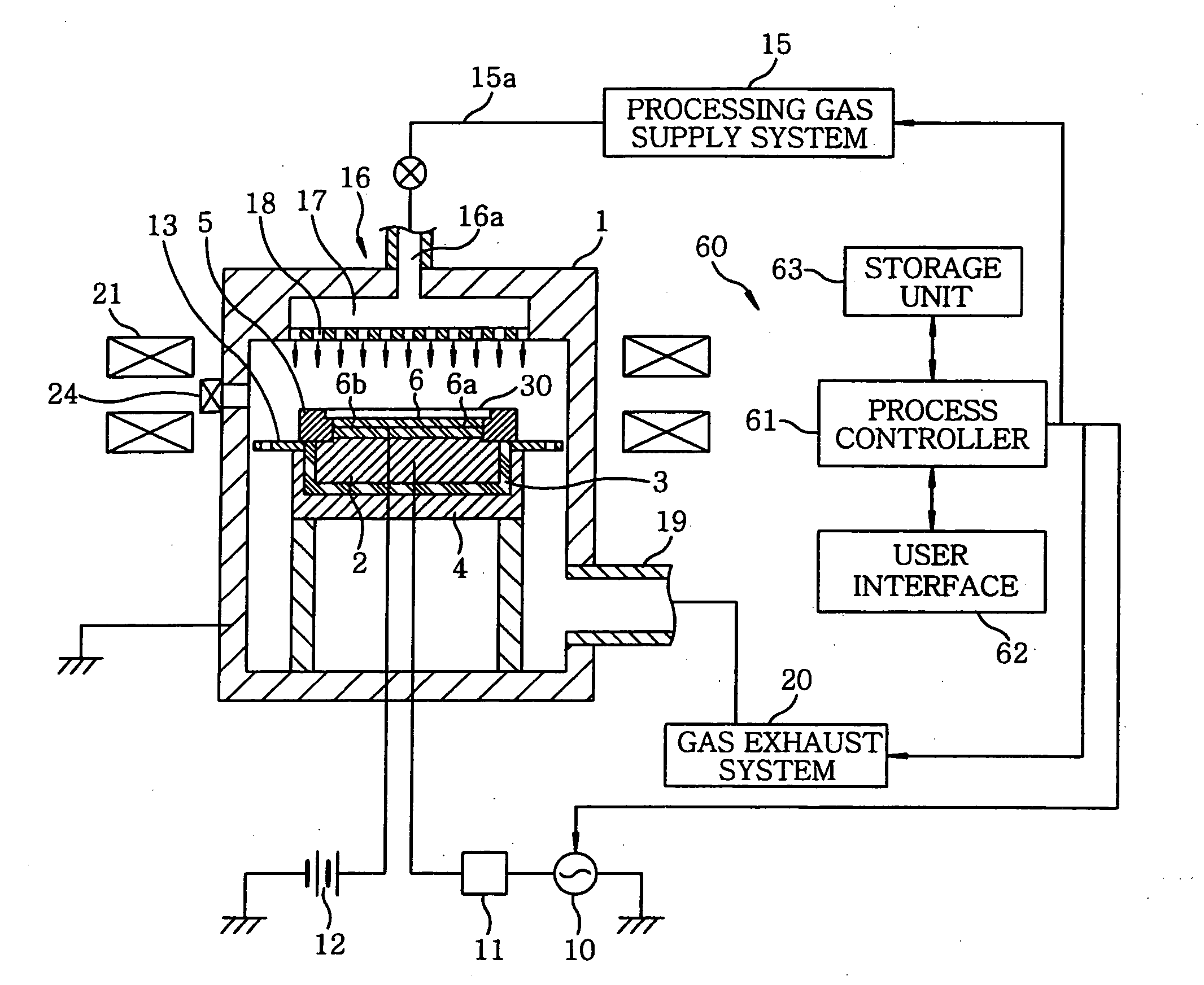
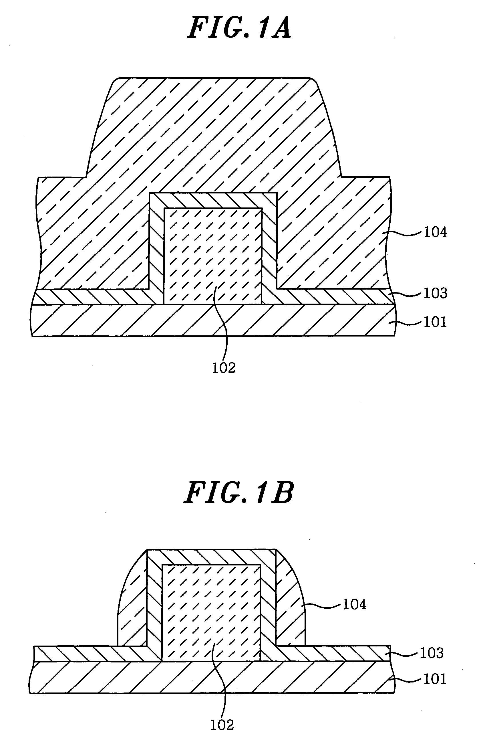
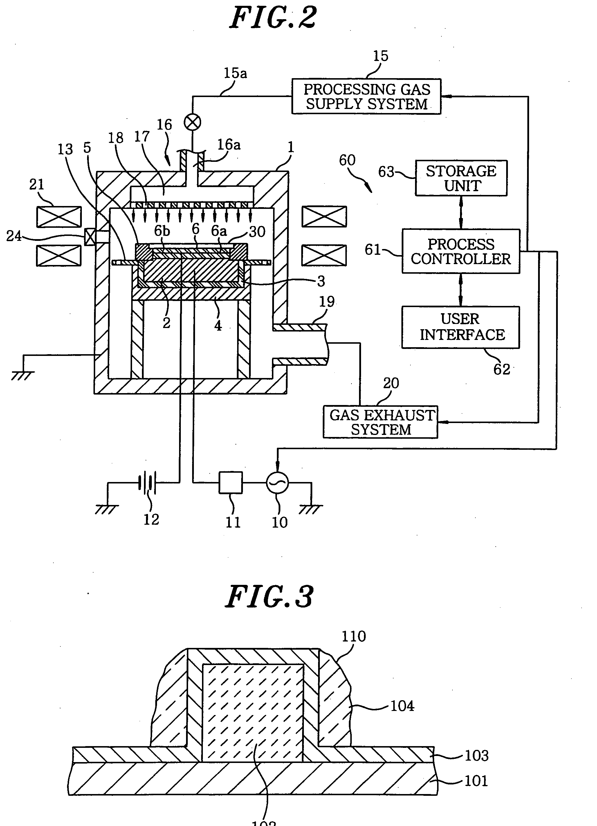
[0021] Hereinafter, a preferred embodiment of the present invention will be described with reference to the accompanying drawings. FIG. 1 is an enlarged sectional view of a semiconductor wafer which is used as a substrate to be processed in a semiconductor device manufacturing method in accordance with the preferred embodiment of the present invention. Further, FIG. 2 illustrates a configuration of a plasma etching apparatus employed as a semiconductor device manufacturing apparatus in accordance with the preferred embodiment of the present invention. The configuration of the plasma etching apparatus will be first described with reference to FIG. 2.

[0022] The plasma etching apparatus includes an airtightly sealed chamber 1 which is electrically grounded. The chamber 1 is of a cylindrical shape, and it is formed of, for example, aluminum. Installed in the chamber 1 is a supporting table 2 for horizontally supporting a semiconductor wafer 30 to be processed. The supporting table 2 is...


PUM

PropertyMeasurementUnit
Fractionaaaaaaaaaa
Fractionaaaaaaaaaa
Fractionaaaaaaaaaa

Abstract

A semiconductor device manufacturing method includes a plasma etching process for selectively plasma etching a silicon nitride film against a silicon oxide film formed under the silicon nitride film in a substrate to be processed. The plasma etching process uses an etching gas including a CmFn gas (m, n represent integers of 1 or greater) added to a gaseous mixture of a CHxFy gas (x, y represent integers of 1 or greater) and O2 gas, wherein the flow rate of the CmFn gas is not greater than 10% of that of the O2 gas. The etching gas may further include a rare gas.

Description

FIELD OF THE INVENTION [0001] The present invention relates to a semiconductor device manufacturing method including a process for selectively plasma etching a silicon nitride film against a silicon oxide film, a semiconductor device manufacturing apparatus, a control program and a computer-readable storage medium storing the control program. BACKGROUND OF THE INVENTION [0002] Conventionally, a manufacturing process for a semiconductor device involves a processing step for selectively plasma etching a silicon nitride film such as a SiN film against an underlying silicon oxide film such as a SiO2 film or a SiOC film (carbon-added silicon oxide film). In this regard, there has been known a technique for improving the selectivity of the silicon nitride film against the silicon oxide film (the ratio of an etching rate of the silicon nitride film to an etching rate of the silicon oxide film) by using a gaseous mixture of, e.g., CH3F and O2 as an etching gas (see, for example, Japanese Pa...

Claims


Application Information

Patent Timeline
IPC IPC(8): H01L21/20H01L21/302
CPCH01L21/31116H01L21/67069
Inventor NARISHIGE, KAZUKI
Owner TOKYO ELECTRON LTD
Why Eureka
Try Eureka