Hybrid memory system for a microcontroller

a memory system and microcontroller technology, applied in the field of digital circuits, can solve the problems of affecting the design cycle and time to market of the asic, wasting expensive silicon real estate, and modifying the instructions in the program memory or the combined program and data memory (e.g., for testing and debugging purposes), so as to eliminate the waste of expensive silicon real estate and maximize the use of memory

Inactive Publication Date: 2007-05-10
ATMEL CORP
View PDF11 Cites 7 Cited by
  • Summary
  • Abstract
  • Description
  • Claims
  • Application Information

AI Technical Summary

Benefits of technology

[0014] Implementations may provide one or more of the following advantages. During test and evaluation of a microcontroller, evaluation patch code can be loaded into the elastic shared RAM array which permits the testing, evaluation, and debug process of the microcontroller (and associated ASIC) to continue without the necessity of waiting for new ROM masks and wafers to be created and processed through a fab. Accordingly, a programmer can load and execute new code from the elastic shared RAM array and, in addition, a portion of the elastic shared RAM array can be used to store data. Depending upon the configuration and the size of individual RAM memories within the elastic shared RAM array, once a microcontroller has been finalized for production, the programmer can set the amount of memory within the elastic shared RAM array to be used to store instructions and data, thus maximizing the usage of memory and eliminating the waste of expensive silicon real estate.

Problems solved by technology

Typically, in application-specific integrated circuits (ASICs) that use an embedded microcontroller having either only a program memory and a data memory (e.g., in accordance with the Harvard architecture) or only a single combined program and data memory (e.g., in accordance with the Von Neumann architecture), modifying the instructions (e.g., for testing and debugging purposes) within the program memory or the combined program and data memory (each of which is typically a read-only memory (ROM)) is generally a difficult task.
Consequently, the design cycle and time to market of the ASIC are affected due to the turn around time needed to re-spin the ASIC.
Also, it is generally expensive to re-spin an ASIC, especially when state of the art masks are used in the re-spin process.
One disadvantage of including an extra RAM memory within a microcontroller design is that the extra RAM memory generally takes up valuable die space or silicon real estate.
Once instruction code within a ROM has been finalized, an ASIC typically goes into production having the extra RAM memory still occupying the (expensive) silicon real estate, and because the extra RAM memory is generally only used for testing and debugging purposes, the extra RAM memory is typically goes unused during normal operation of the ASIC.
As production quantities of ASICs increase, cumulatively, the extra area taken up by the extra RAM memory generally become more expensive relative to using methods of re-spinning new ASICs to debug and test ASICs.

Method used


Image

  • Hybrid memory system for a microcontroller
  • Hybrid memory system for a microcontroller
  • Hybrid memory system for a microcontroller

Examples


Embodiment Construction

[0030] The present invention relates generally to digital circuits, and more particularly to memory systems in a microcontroller. The following description is presented to enable one of ordinary skill in the art to make and use the invention and is provided in the context of a patent application and its requirements. Various modifications to the preferred implementations and the generic principles and feature described herein will be readily apparent to those skilled in the art. Thus, the present invention is not intended to be limited to the implementations shown but is to be accorded the widest scope consistent with the principles and features described herein.

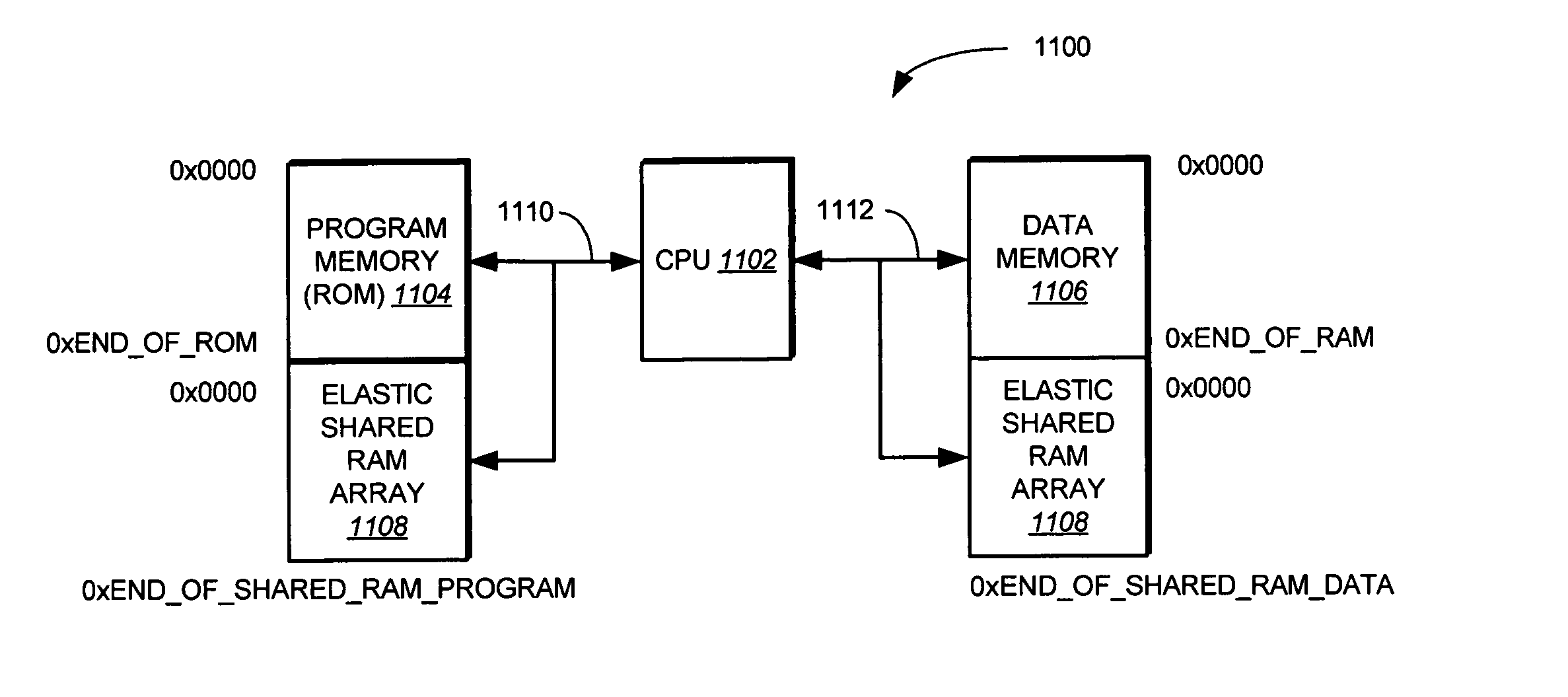
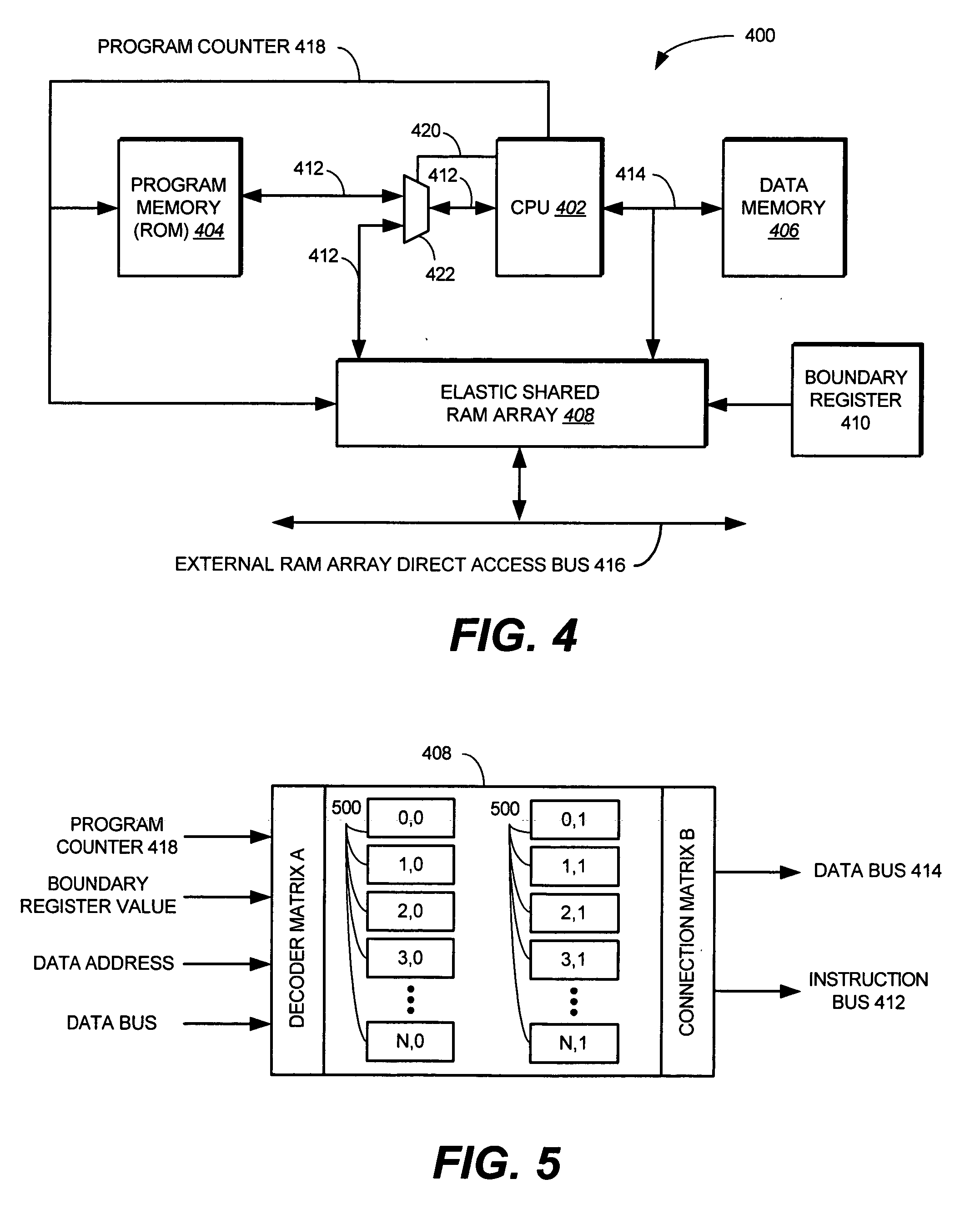
[0031]FIG. 1 shows a block diagram of a microcontroller 400. In one implementation, microcontroller 400 is a ROM based Harvard 8-bit data, 16-bit instruction microcontroller. Microcontroller 400 includes a CPU 402, a program memory 404, a data memory 406, an elastic shared ram array 408, and a boundary register 410. CPU 402...


PUM


Abstract

A microcontroller, system and method are provided. In one implementation, a microcontroller is provided that includes a first memory operable to store instructions for normal operational use of the microcontroller, a second memory operable to store patch code instructions during debugging of the instructions within the first memory, and a central processing unit (CPU) operable to fetch instructions from the first memory and the patch code instructions from the second memory. The second memory is further operable to store the instructions for normal operational use of the microcontroller or data after the debugging of the instructions within the first memory is completed.

Description

FIELD OF THE INVENTION [0001] The present invention relates generally to digital circuits, and more particularly to memory systems in a microcontroller. BACKGROUND OF THE INVENTION [0002] A microcontroller is generally a computer-on-a-chip optimized to control electronic devices. A microcontroller typically includes a central processing unit (CPU), a random access memory (RAM), a read-only memory (ROM), input / output (I / O) ports, and timers. Unlike a general-purpose computer, which also includes similar components, a microcontroller is usually designed to implement a very specific task—e.g., to control a particular system. As a result, the components of a microcontroller can be simplified and reduced, which cuts down on production costs. Several architectures exist for microcontrollers. Two architectures in particular are the Harvard architecture and the Von Neumann architecture. [0003]FIG. 1 shows a microcontroller 100 in accordance with the Harvard architecture. Microcontroller 100...

Claims


Application Information

Patent Timeline
Patent Type & Authority Applications(United States)
IPC IPC(8): G06F9/44
CPCG06F9/328G06F9/3802
Inventor BRACAMONTES, ROCENDO
Owner ATMEL CORP
Why Eureka
Try Eureka