Printed circuit board using paste bump and manufacturing method thereof

a technology of printed circuit boards and bumps, which is applied in the direction of printed circuits, printed circuit details, printed elements, etc., can solve the problems of difficult micro-circuit formation, high cost, time-consuming, complicated plating process, etc., and achieves improved heat-releasing effect, improved connection reliability, and reduced lead times

Inactive Publication Date: 2007-05-17
SAMSUNG ELECTRO MECHANICS CO LTD
View PDF3 Cites 17 Cited by
  • Summary
  • Abstract
  • Description
  • Claims
  • Application Information

AI Technical Summary

Benefits of technology

[0014] The present invention aims to provide a printed circuit board and a manufacturing method thereof, with which a multilayer printed circuit board is formed by collectively stacking a core board having plated BVH's, a board having paste bumps printed on a core board, and a paste bump board, to implement a structurally stable all-layer IVH structure, improve the connection reliability by means of an increase in interlayer connection area, and reduce lead times. Another object of the present invention is to provide a printed circuit board using paste bumps and a manufacturing method thereof, for which paste bump boards are stacked on a core board and paste bumps are filled in heat-releasing holes, such that the heat-releasing effect is improved.

Problems solved by technology

However, the conventional manufacturing process for multilayer printed circuit boards is unable to comply to requests for low costs according to lowering prices in the applied products (e.g. cell phones, etc.) and requests for reduced lead times for increased productivity, and thus there is a demand for a new manufacturing process that can resolve such problems.
Also, the conventional method requires a plating process which is complicated, expensive, and time-consuming, and does not provide a sufficient heat-releasing effect through the PTH's.
Also, when forming circuit patterns after forming the plating layer, the conventional method presents difficulties in forming micro circuits, caused by the increase in thickness of the circuit patterns due to the plating layer.
Also, there is a likelihood of short circuits occurring in a high-voltage, high-frequency environment, and there are paste bumps filled in the board's via holes so that the properties of heat release through PTH's have not been improved.

Method used


Image

  • Printed circuit board using paste bump and manufacturing method thereof
  • Printed circuit board using paste bump and manufacturing method thereof
  • Printed circuit board using paste bump and manufacturing method thereof

Examples


Embodiment Construction

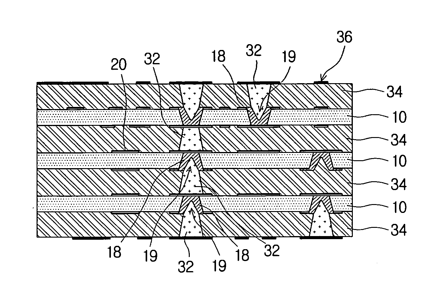
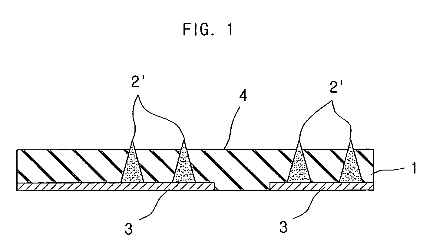
[0051] Embodiments of the printed circuit board using paste bumps and manufacturing method thereof, according to aspects of the invention, will be described below in more detail with reference to the accompanying drawings. In the description with reference to the accompanying drawings, those components are rendered the same reference number that are the same or are in correspondence regardless of the figure number, and redundant explanations are omitted.

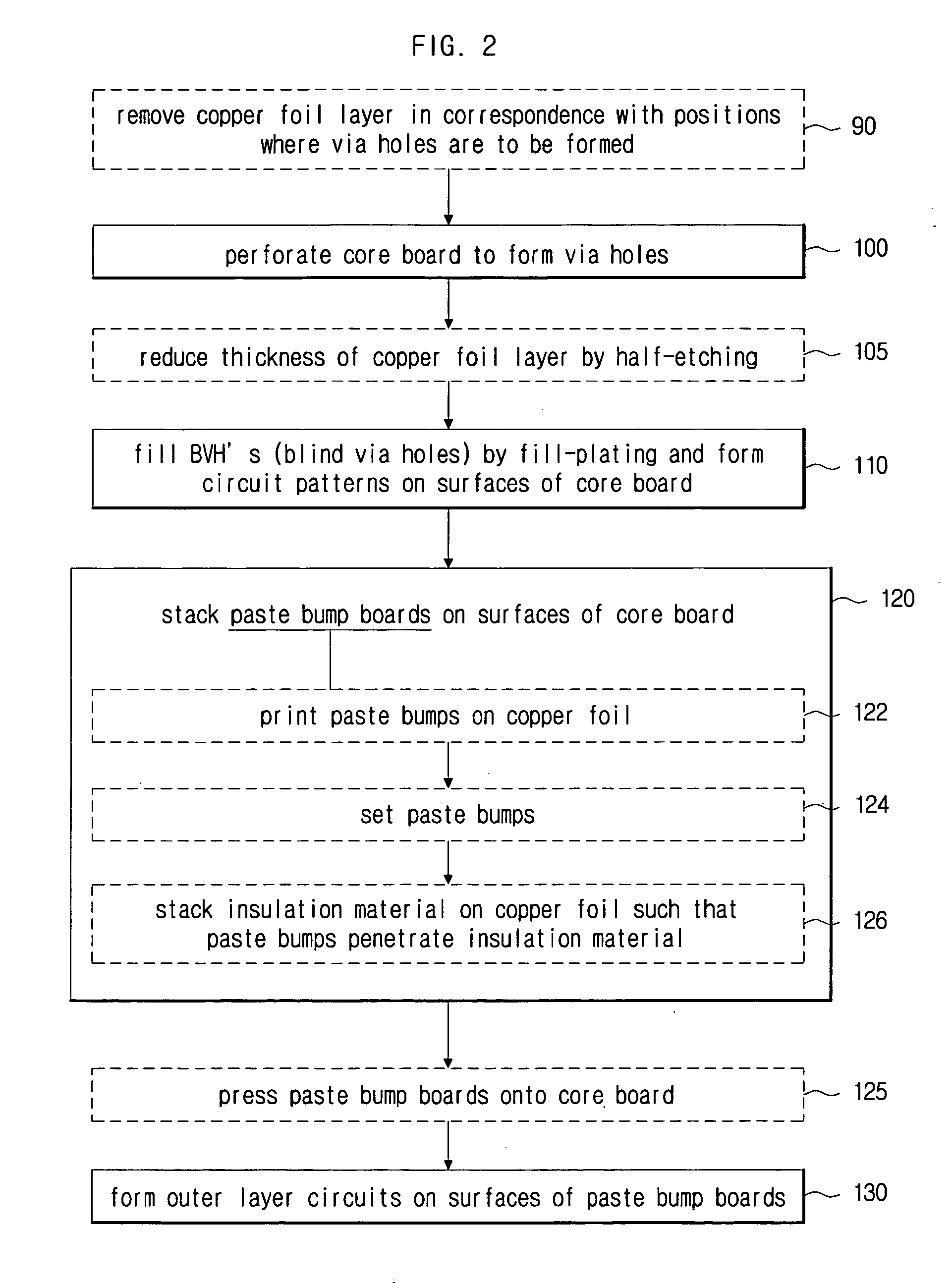
[0052]FIG. 2 is a flowchart illustrating a method of manufacturing a printed circuit board using paste bumps according to an embodiment of the present invention.

[0053] The present invention is for reducing the manufacture costs and times of a multilayer printed circuit board by collectively stacking paste bump boards on a core board, where a paste bump board is formed by performing plating on BVH's (blind via holes) formed in a core board, printing paste bumps on a copper foil in correspondence with the positions of the BVH's, and ...


PUM

PropertyMeasurementUnit
thicknessaaaaaaaaaa
strengthaaaaaaaaaa
electricallyaaaaaaaaaa

Abstract

A printed circuit board using paste bumps and manufacturing method thereof are disclosed. With the method of manufacturing a printed circuit board using paste bumps, comprising: (a) perforating a core board to form at least one via hole, (b) filling the at least one via hole by fill-plating and forming a circuit pattern on at least one surface of the core board, (c) stacking a paste bump board on at least one surface of the core board, and (d) forming an outer layer circuit on a surface of the paste bump board, a structurally stable all-layer IVH structure can be implemented due to increased strength in the BVH's of the plated core boards, the manufacture time can be reduced due to parallel processes and collective stacking, implementing micro circuits can be made easy due to the copper foils of the paste bump boards stacked on the outermost layers, the manufacture costs can be reduced as certain plating and drilling processes may be omitted, the interlayer connection area is increased between circuit patterns for improved connection reliability, and dimple coverage can be obtained.

Description

CROSS-REFERENCE TO RELATED APPLICATIONS [0001] This application claims the benefit of Korean Patent Application No. 2005-0109850, filed with the Korean Intellectual Property Office on Nov. 16, 2005, and Korean Patent Application No. 2005-0109855 filed on Nov. 16, 2005, the disclosures of which are incorporated herein by reference in their entirety. BACKGROUND [0002] 1. Technical Field [0003] The present invention relates to a printed circuit board, and in particular, to a printed circuit board using paste bumps and a manufacturing method thereof. [0004] 2. Description of the Related Art [0005] The conventional multilayer printed circuit board is manufactured by forming inner layer circuits on the surface of a core board, such as a copper clad laminate (CCL), etc., through the application of an additive process or a subtractive process, etc., and by forming outer layer circuits through the stacking of insulation layers and metal layers in order, by the same method as for the inner la...

Claims


Application Information

Patent Timeline
Patent Type & Authority Applications(United States)
IPC IPC(8): H05K1/11H01R12/04
CPCH05K3/4069H05K3/462H05K3/4647H05K3/4652H05K2201/0355Y10T29/49155H05K2201/09536H05K2201/096H05K2203/0353H01R12/523H05K2201/09509
Inventor MOK, JEE-SOORYU, CHANG-SUPLEE, EUNG-SUEKSEO, YOUN-SOOSHIN, HEE-BUMOH, YOONGSEO, BYUNG-BAEKIM, TAE-KYOUNGPARK, DONG-JIN
Owner SAMSUNG ELECTRO MECHANICS CO LTD
Why Eureka
Try Eureka