Semiconductor integrated circuit device

a technology of integrated circuit and semiconductor, which is applied in the direction of pulse generator, pulse technique, instruments, etc., can solve the problems of increasing subthreshold leakage current, affecting the operation of the device, so as to achieve the effect of reducing power consumption during standby, and substantially minimizing leakage curren

Inactive Publication Date: 2007-05-17
RENESAS ELECTRONICS CORP
View PDF7 Cites 29 Cited by
  • Summary
  • Abstract
  • Description
  • Claims
  • Application Information

AI Technical Summary

Benefits of technology

[0015] According to an aspect of the present invention, there is provided a semiconductor integrated circuit device including a field effect transistor, and a voltage control circuit generating a control voltage to be supplied to a gate terminal of the field effect transistor for deactivating the field effect transistor. The voltage control circuit controlling a voltage so as to substantially minimize leakage current which flows when the field effect transistor is inactive in accordance with a device temperature.
[0016] In this semiconductor integrated circuit device, a control voltage is controlled in accordance with a device temperature so that the leakage current which flows when a field effect transistor is inactive is substantially minimal. This enables the leakage current to be substantially minimized regardless of a device temperature. As a result, power consumption during standby can be substantially minimized irrespective of a temperature in the semiconductor integrated circuit device.

Problems solved by technology

Further, in recent semiconductor integrated circuit device, not only the power consumption during the active state but also the power consumption during the standby state pose a problem.
An increase in the power consumption during the standby state is incurred by the smaller geometry semiconductor process technology and the lower power supply voltage particularly in a MISFET (Metal Insulator Semiconductor Field Effect Transistor).
The low threshold voltage causes an increase in subthreshold leakage current.
Further, the smaller geometry semiconductor process technology causes a gate insulating layer to be thinner, which leads to an increase in leakage current.
The increase in the leakage current raises the drawbacks such as an increase in the power consumption during standby of the semiconductor integrated circuit device and reduction of a data maintain period of a memory cell using a MISFET (e.g. DRAM cell).
Although the above techniques provide control of a gate voltage or a source voltage so as to reduce leakage current, they do not provide control in accordance with temperature.
Therefore, although the above techniques can reduce leakage current when the semiconductor integrated circuit device is at an ambient temperature, for example, the leakage current undesirably increases when the temperature becomes higher.
Further, if an absolute value of the negative voltage of the gate voltage is large, much time and energy are required to increase the gate voltage to a power supply voltage.
This hinders high-speed access to a memory cell, for example.

Method used


Image

  • Semiconductor integrated circuit device
  • Semiconductor integrated circuit device
  • Semiconductor integrated circuit device

Examples


first embodiment

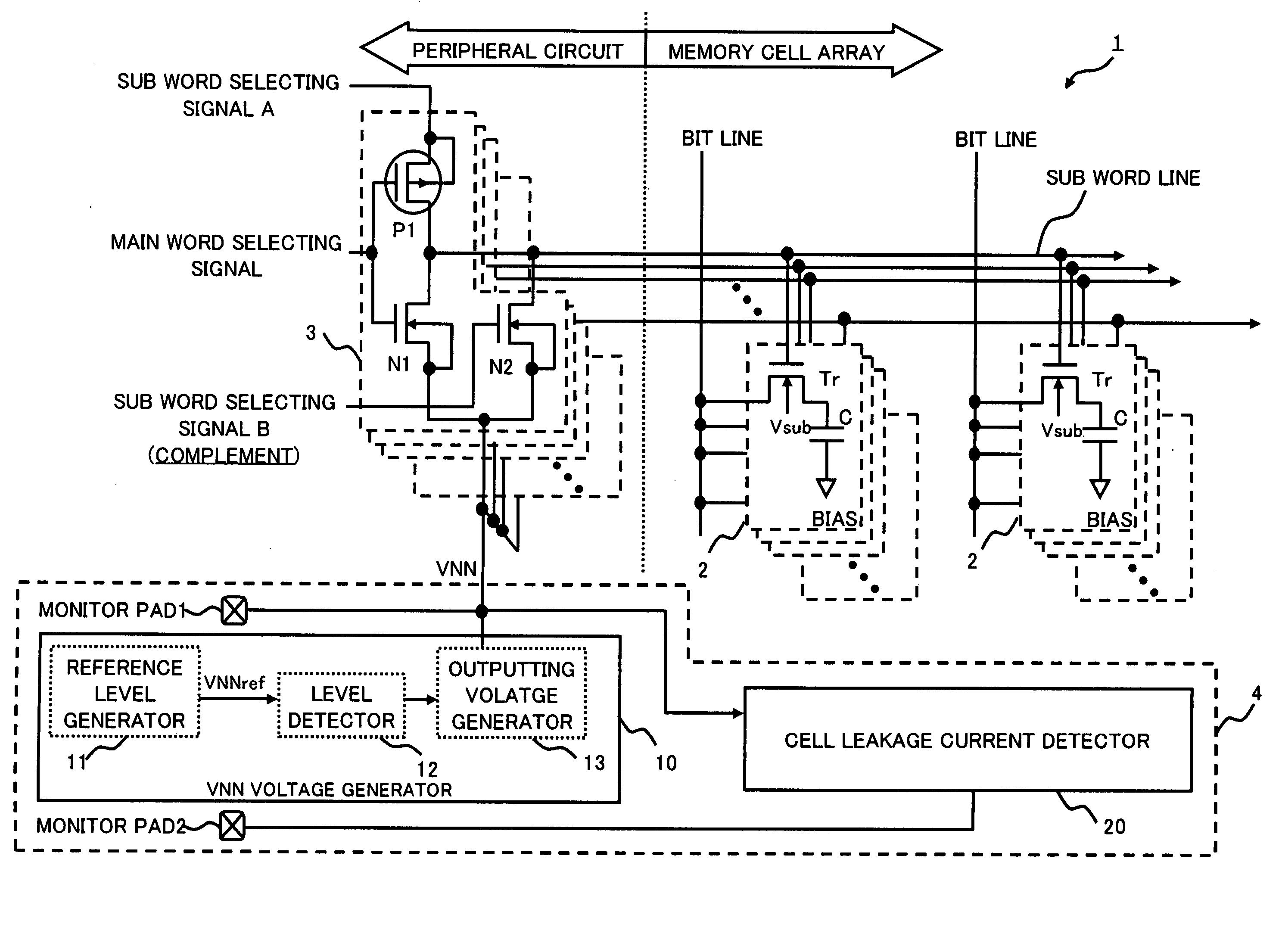
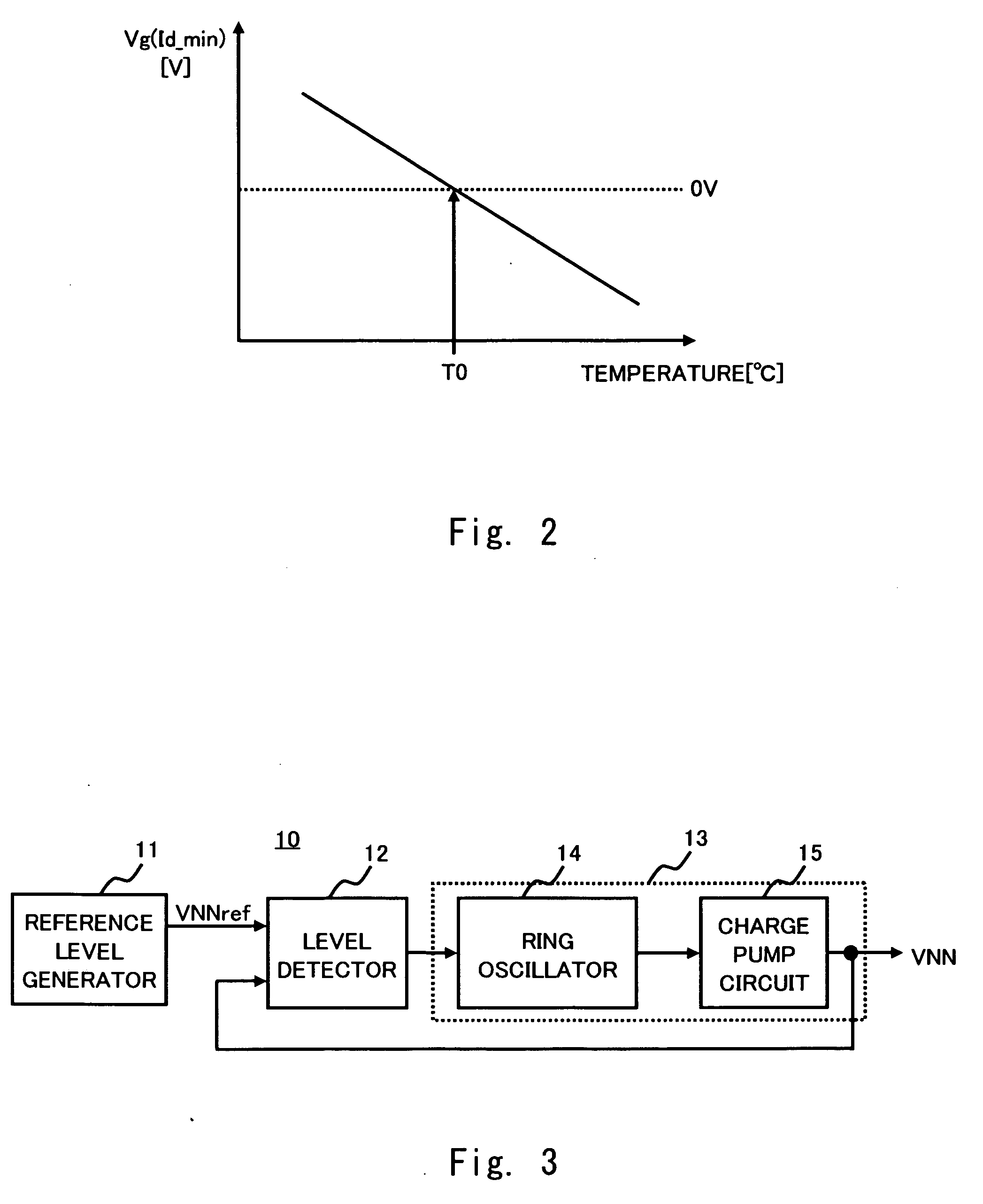
[0038] Exemplary embodiments of the present invention are described hereinafter with reference to the drawings. A semiconductor integrated circuit device of the present invention controls a gate voltage in accordance with a temperature so as to substantially minimize the leakage current of a field effect transistor (e.g. MISFET) which is formed on a semiconductor substrate (referred to hereinafter simply as the substrate). In the exemplary embodiments described below, a DRAM is used as an example of a semiconductor integrated circuit device, and the control of a gate voltage of a transfer transistor of the DRAM is described in detail by way of illustration. The leakage current in the following description refers to the leakage current as described earlier.

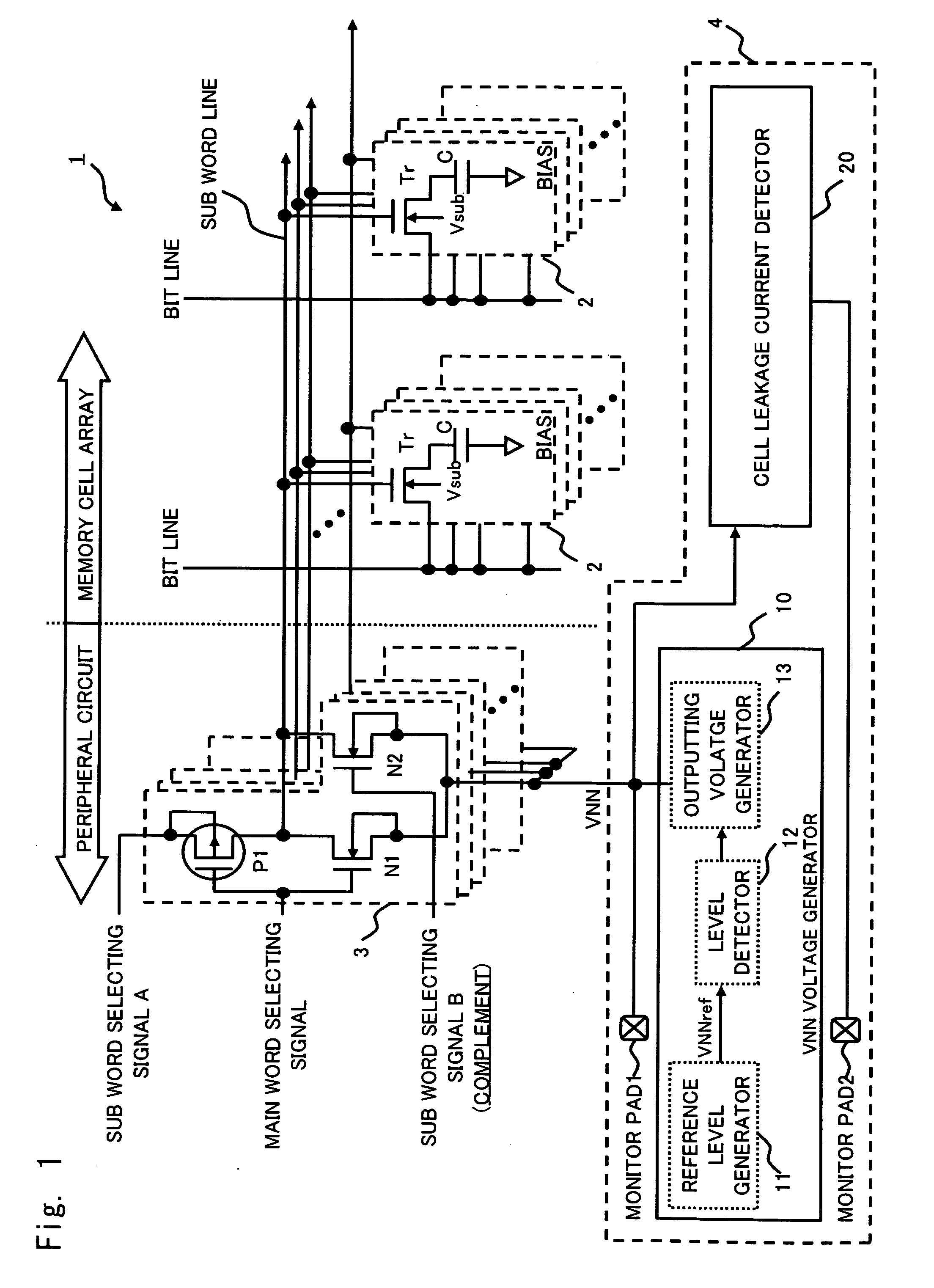
[0039]FIG. 1 shows a DRAM 1 according to a first embodiment of the invention. As shown in FIG. 1, the DRAM 1 includes a plurality of memory cells 2, bit lines and sub word lines in a memory cell array, and sub word line voltage se...

second embodiment

[0072] The voltage control circuit 4 according to the first embodiment measures the value of the control voltage VNN at which the leakage current is minimal by the cell leakage current detector 20 and sets the initial value of the control voltage VNN based on the measurement result. On the other hand, a voltage control circuit 4a according to a second embodiment of the invention measures the leakage current during the operation of the DRAM and reflects the measurement result to the value of the control voltage VNN. Thus, the voltage control circuit 4a of the second embodiment implements the automatic control of the value of the control voltage VNN.

[0073] The voltage control circuit 4a is described in detail hereinafter. FIG. 10 is a block diagram showing the voltage control circuit 4a. As shown in FIG. 10, the voltage control circuit 4a includes a second cell leakage current detector (e.g. cell leakage current detector 20b), a level shifter 30, and a comparator 40 in addition to th...

third embodiment

[0080] A level detector 12a according to a third embodiment of the present invention is such that the comparing voltage generator 122 of the first embodiment is replaced with a comparing voltage generator 122a of the third embodiment. The comparing voltage generator 122 of the first embodiment determines the values of the resistors R122 and R123 at the time of design. On the other hand, the comparing voltage generator 122a of the third embodiment can adjust the values of the resistors R122 and R123 before shipment by laser trimming, for example, in addition to determining the values of the resistors R122 and R123 in design. The same blocks as in the first embodiment are denoted by the same reference symbols and not particularly described herein.

[0081]FIG. 12 is a circuit diagram of the level detector 12a according to the third embodiment. As shown in FIG. 12, in the level detector 12a of the third embodiment, a voltage dividing element 123a is connected between the terminal to inpu...


PUM


Abstract

The semiconductor integrated circuit device includes a voltage control circuit that generates a control voltage for deactivating a field effect transistor by a gate voltage. The voltage control circuit controls a voltage so as to substantially minimize the leakage current which flows when the field effect transistor is inactive with respect to a device temperature.

Description

BACKGROUND OF THE INVENTION [0001] 1. Field of the Invention [0002] The present invention relates to a semiconductor integrated circuit device and, particularly, to a semiconductor integrated circuit device which reduces leakage current by controlling a gate voltage in view of the temperature characteristics of the leakage current flowing when a field effect transistor is inactive. [0003] 2. Description of Related Art [0004] In recent semiconductor integrated circuit devices, power consumption decreases along with decreasing power supply voltage while it increases at the same time along with increasing degree of integration and increasing access speed with the advent of the smaller geometry semiconductor process technology. Further, in recent semiconductor integrated circuit device, not only the power consumption during the active state but also the power consumption during the standby state pose a problem. An increase in the power consumption during the standby state is incurred by...

Claims


Application Information

Patent Timeline
Patent Type & Authority Applications(United States)
IPC IPC(8): H02H9/00
CPCG11C5/14
Inventor SHIMOGAWA, KENJYUFURUTA, HIROSHI
Owner RENESAS ELECTRONICS CORP
Why Eureka
Try Eureka