Wafer redistribution structure with metallic pillar and method for fabricating the same

Inactive Publication Date: 2007-05-17
ADVANCED SEMICON ENG INC
View PDF3 Cites 11 Cited by
  • Summary
  • Abstract
  • Description
  • Claims
  • Application Information

AI Technical Summary

Benefits of technology

[0011] It is therefore an object of the invention to provide a redistribution structure of a wafer structure and a method of fabricating the same. The design adopts a multi-layered redistribution structure, avoiding the occurrences of

Problems solved by technology

Furthermore, the redistribution layers of the redistribution

Method used


Image

  • Wafer redistribution structure with metallic pillar and method for fabricating the same
  • Wafer redistribution structure with metallic pillar and method for fabricating the same
  • Wafer redistribution structure with metallic pillar and method for fabricating the same

Examples


Example

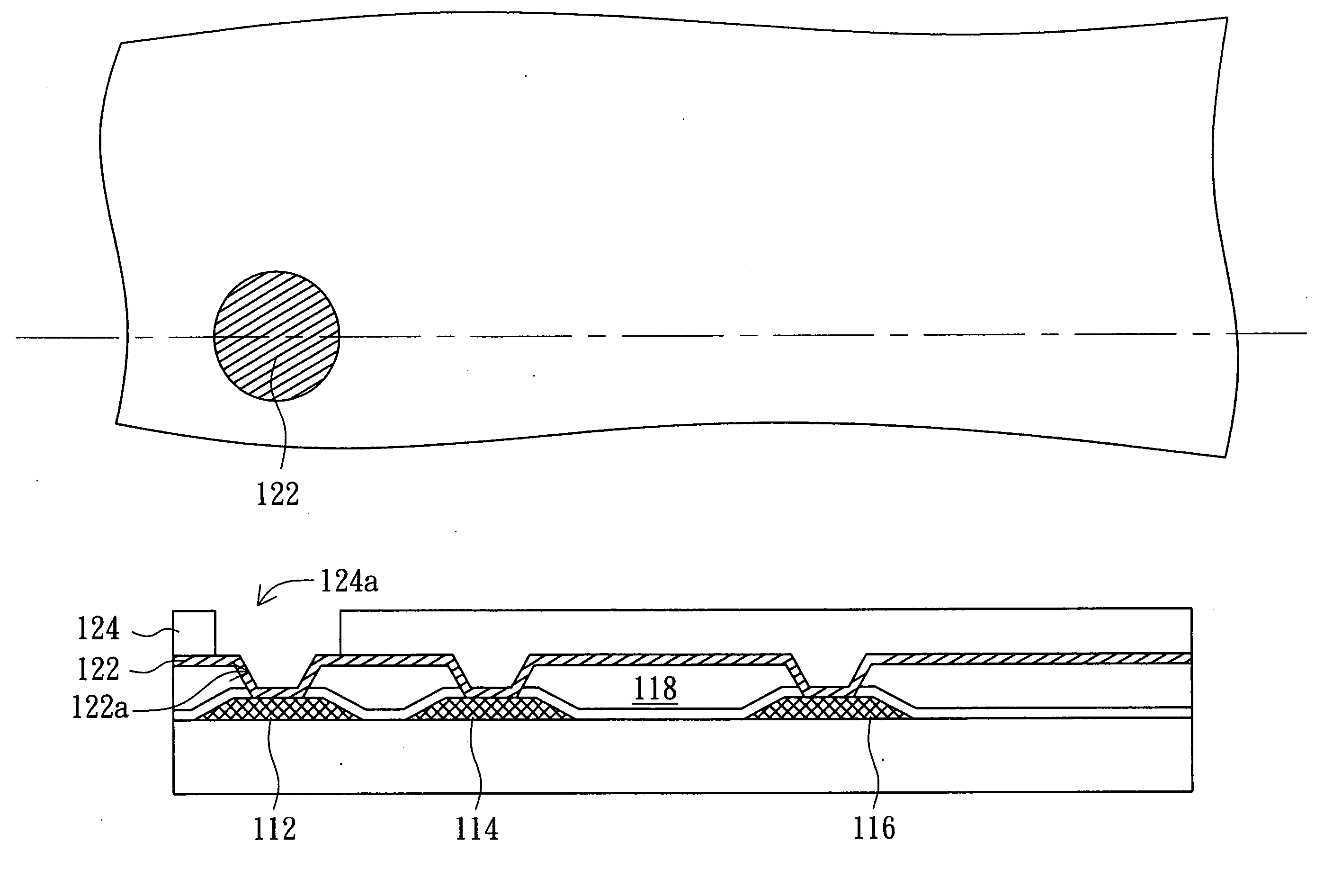
[0021] The invention provides a multi-layered redistribution structure and a method for fabricating the same, avoiding the occurrences of short-circuits even when circuits are crisscrossed. According to the invention, the bumps have the same height and are without height drop. At the contact point of the redistribution layer extended from the original position of the solder pad, a metallic pillar is used to fill the indented portion and elevate the under bump metallurgy (UBM) layer, so that the bump extended from the original position of the solder pad has the same height with the bump positioned elsewhere.

[0022] Referring to FIG. 3, a cross-sectional view of a wafer structure according to a preferred embodiment of the invention is shown. The wafer structure 100 of the present embodiment of the invention includes a substrate 110, a redistribution structure 234, a third passivation layer 170, an under bump metallurgy layer (UBM) 180 and a bump 190. The substrate 110 has a solder pad...


PUM


Abstract

A wafer structure and a method for fabricating the same are provided. The wafer structure comprises a substrate, a redistribution structure, a passivation layer, an under bump metallurgy (UBM) layer and a bump. The substrate has a solder pad. The redistribution structure is formed on the substrate and comprises a copper pillar electrically connected to the solder pad. The passivation layer is formed on the redistribution structure and has an aperture to expose the copper pillar. The UBM layer is formed in the aperture and disposed on the copper pillar. The bump is formed on the UBM layer.

Description

[0001] This application claims the benefit of Taiwan application Ser. No. 94140168, filed Nov. 15, 2005, the subject matter of which is incorporated herein by reference. BACKGROUND OF THE INVENTION [0002] 1. Field of the Invention [0003] The invention relates in general to a wafer structure and a method for fabricating the same, and more particularly to a redistribution structure of a wafer structure and a method for fabricating the same. [0004] 2. Description of the Related Art [0005] In response to the requirements with regards to the integration and miniaturization of electronic devices, the packaging technology of integrated circuits (ICs) is headed towards miniaturization and high density. Examples of the packaging technology of high-density integrated circuits including the ball grid array (BGA) technology, the chip-scale package (CSP) technology, the flip chip (F / C) technology, and the multi-chip module (MCM) technology are provided. In terms of a high-density integrated circ...

Claims


Application Information

Patent Timeline
IPC IPC(8): H01L21/44H01L23/48
CPCH01L24/03H01L24/05H01L24/06H01L24/11H01L2224/0401H01L2224/1147H01L2224/13099H01L2224/131H01L2924/01005H01L2924/01013H01L2924/01022H01L2924/01028H01L2924/01029H01L2924/01042H01L2924/01074H01L2924/01078H01L2924/014H01L2924/14H01L2924/00014H01L24/13H01L2924/01006H01L2924/01023H01L2924/01024H01L2224/05555H01L2224/05001H01L2224/0554H01L2224/023H01L2924/0001
Inventor LO, JIAN-WEN
Owner ADVANCED SEMICON ENG INC
Why Eureka
Try Eureka