Light-emitting device and electronic apparatus

a technology of light-emitting devices and electronic devices, which is applied in the direction of thermoelectric devices, electroluminescent light sources, electric lighting sources, etc., can solve the problems of cracks or peeling of gas barrier layers, cracks due to stress concentration, and sealing properties, etc., to improve the sealing properties of plurality, small covering regions, and large covering regions

Active Publication Date: 2007-05-24
SEIKO EPSON CORP
View PDF7 Cites 39 Cited by
  • Summary
  • Abstract
  • Description
  • Claims
  • Application Information

AI Technical Summary

Benefits of technology

[0015] According to this light-emitting device, the first organic buffer layer, which is a lower layer and has a small covering region, is thicker than the second organic buffer layer, which is an upper layer and has a large covering region. Therefore, even when the total thickness of the first and second organic buffer layers sufficiently increases in order to improve the sealing property of a plurality of light-emitting elements, the rise angle of the gas barrier layer is equal to the angle of the second edge portion of the second organic buffer layer having a smaller thickness. Since the first constant portion and the first edge portion overlap the second constant portion, the gas barrier layer is sequentially arranged along the second edge portion and the first edge portion in the rising portion thereof. Therefore, even when the thickness of the first organic buffer layer, which is an upper layer and a small size, is large and the angle of the first edge portion is large, the gas barrier layer gradually rises. In this way, it is possible to sufficiently increase the total thickness of the first and second organic buffer layers covering a region in which the plurality of light-emitting elements are arranged, while slightly increasing t...

Problems solved by technology

When remarkable stress concentration occurs, the gas barrier layer may be cracked or peeled off.
Accordingly, a crack may occur due to the stress concentration.
If the gas barrier layer cracks or is peeled off, moisture contained in atmospheric air is infiltrated into the organic EL elements, which causes the sealing property (in particular, coatability for minute foreign materials not purified by a clean room) of the organic EL elements to significantly deteriorate.
Linen a gas barrier film is composed of an organic compound film having low elasticity to prevent the stress concentration, or when the gas barrier layer is formed with a constant thickness to prevent the stress concentration, the gas barrier layer...

Method used


Image

  • Light-emitting device and electronic apparatus
  • Light-emitting device and electronic apparatus
  • Light-emitting device and electronic apparatus

Examples


first embodiment

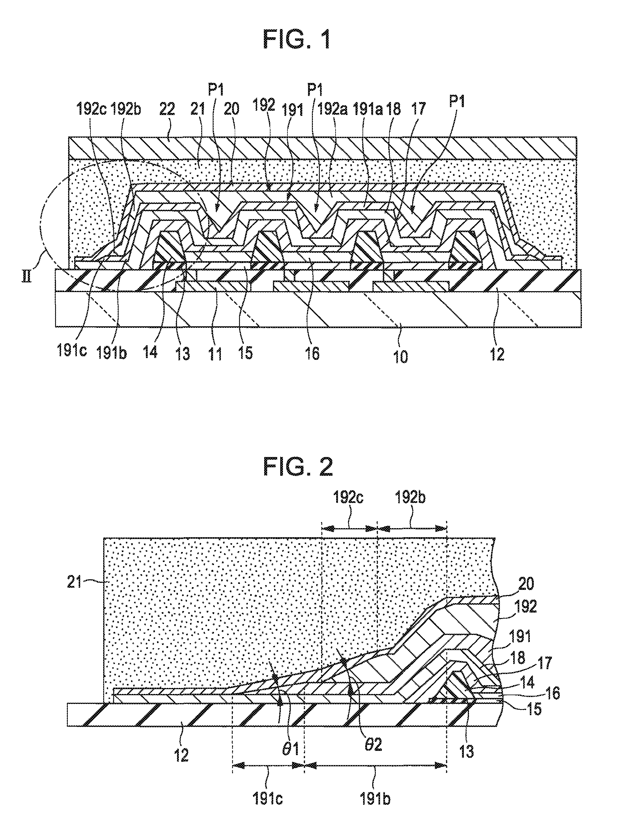
[0036] An organic EL panel (light-emitting device) according to a first embodiment of the invention is a full color panel using a polymer organic EL material, which will be described later. The organic EL panel has an organic EL element emitting a red light component, an organic EL element emitting a green light component, and an organic EL element emitting a blue light component that are arranged side by side and is capable of performing full color display. The organic EL panel is a top emission type in which light from the organic EL element is emitted from the opposite side of a main substrate.

Structure

[0037]FIG. 1 is a cross-sectional view of the organic EL panel. FIG. 2 is an enlarged cross-sectional view illustrating a portion A of the organic EL panel. The organic EL panel includes a flat main substrate 10. The main substrate 10 is formed of, for example, glass or plastic, and has a plurality of organic EL elements P1 formed on the upper surface thereof. The organic EL ele...

second embodiment

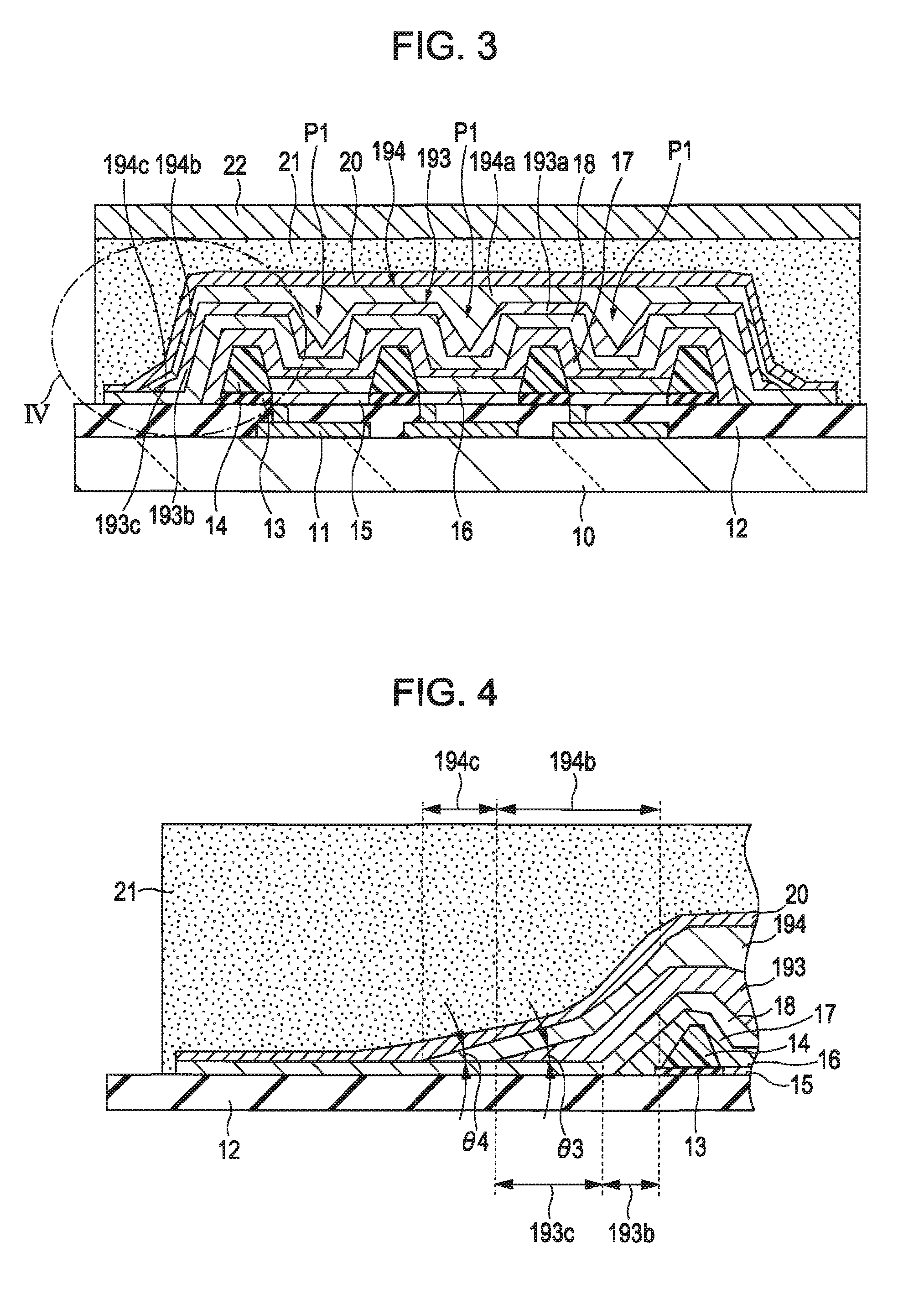
[0064] An organic EL panel according to a second embodiment of the invention is similar to the organic EL panel according the first embodiment except for the structure of an organic buffer layer.

[0065]FIG. 3 is a cross-sectional view of the organic EL panel. FIG. 4 is an enlarged cross-sectional view illustrating a portion B of the organic EL panel. In the organic EL panel, a first organic buffer layer 193 is formed on a cathode protecting layer 18 so as to overlap a plurality of EL elements P1. A second organic buffer layer 194 is formed on the first organic buffer layer 193 so as to cover the first organic buffer layer 193. A gas barrier layer 20 is formed on the cathode protecting layer 18, the first organic buffer layer 193, and the second organic buffer layer 194 so as to cover both the organic buffer layers.

[0066] The first organic buffer layer 193 and the second organic buffer layer 194 are provided to improve the flatness and adhesion of the gas barrier layer 20 and to buf...

third embodiment

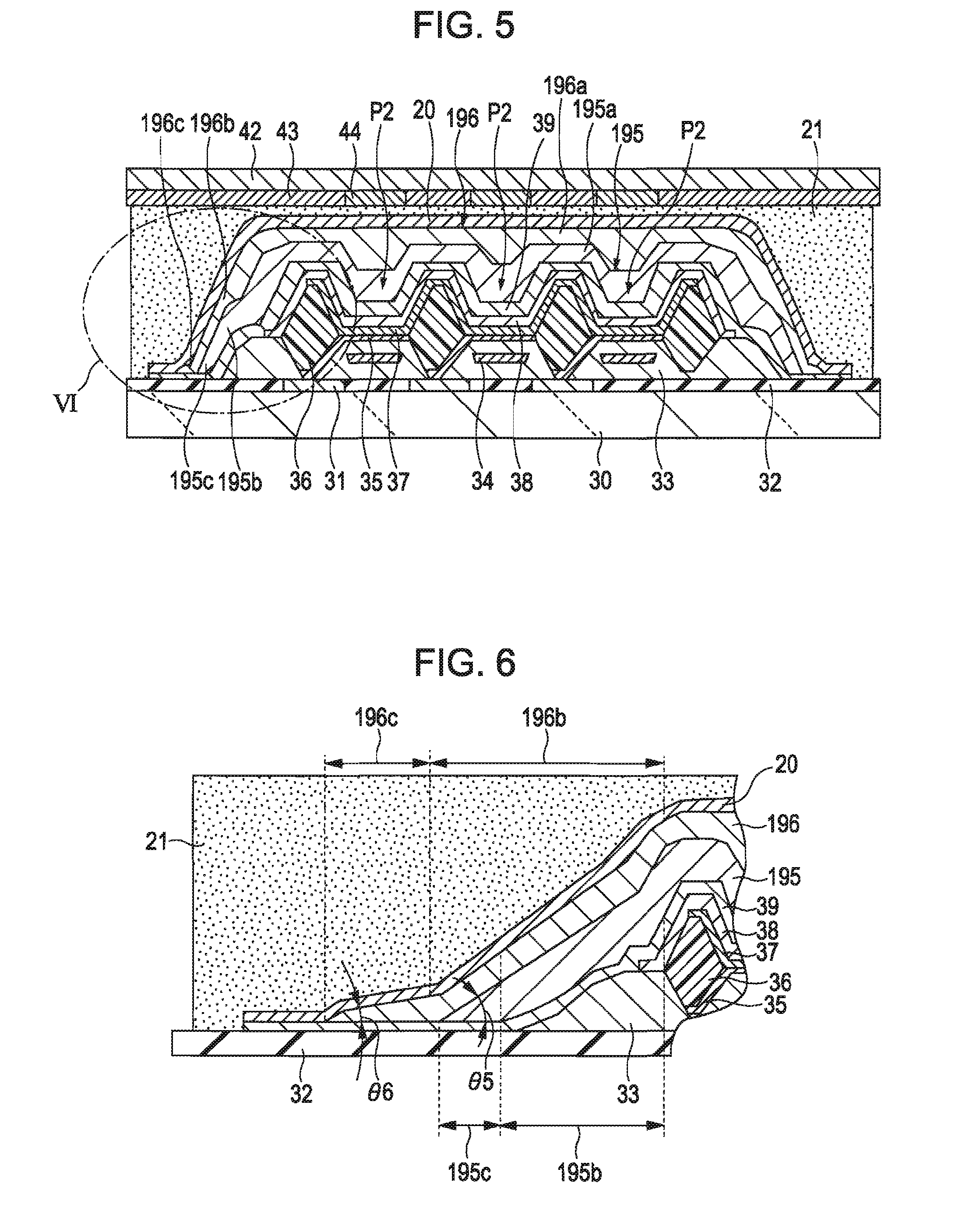
[0075] The structure of an organic buffer layer of an organic EL panel according to a third embodiment of the invention is the same as that of the organic buffer layer of the organic EL panel according to the second embodiment. However, the organic EL panel according to the third embodiment is a full color panel using a low-molecular-weight-based organic EL material, which will be described later, and can perform full color display using organic EL elements emitting white light and color filters.

Structure

[0076]FIG. 5 is a cross-sectional view illustrating the organic EL panel, and FIG. 6 is an enlarged cross-sectional view illustrating a portion C of the organic EL panel. The organic EL panel includes a flat main substrate 30. The main substrate 30 is formed of glass or plastic, and a plurality of organic EL elements P2 are formed on the main substrate 30. The organic EL element P2 is an element that emits white light, has an organic light-emitting layer 37 formed of a low-molecu...


PUM


Abstract

A light-emitting device includes: a substrate; a plurality of light-emitting elements which is formed on the substrate and each of which has an anode partitioned by an insulating pixel partition wall, a cathode, and an organic light-emitting layer interposed therebetween and emits light by an electric field generated by the anode and the cathode; a first organic buffer layer that is formed by applying an organic compound and hardening the organic compound and covers a region larger than the region in which the plurality of light-emitting elements are formed; a second organic buffer layer that is that is formed by applying an organic compound and hardening the organic compound and is arranged above the substrate with the first organic buffer layer interposed therebetween so as to cover the plurality of light-emitting elements; and a gas barrier layer that is formed of an inorganic compound, covers a region larger than the region in which the first and second organic buffer layers are formed, and protects the plurality of light-emitting elements from air. In the light-emitting device, a region of the substrate overlapping the first organic buffer layer is not completely matched with a region of the substrate overlapping the second organic buffer layer.

Description

BACKGROUND [0001] 1. Technical Field [0002] The present invention relates to a technique for sealing a thin film of a light-emitting element. [0003] 2. Related Art [0004] As one type of light-emitting elements, there is an organic EL (electroluminescent) element that has a multilayered structure of two electrodes and a thin organic light-emitting film, formed of an organic compound, interposed between the two electrodes and emits light by excitation due to an electric field generated between the two electrodes. A sealing process is performed to prevent an organic light-emitting material and a cathode, which includes an electron injection layer formed of, for example, calcium, magnesium, or aluminum complex, from deteriorating. As sealing techniques, a thin-film sealing technique for covering organic EL elements with an excessively thin inorganic compound film has been known (see JP-A-9-185994, JP-A-2001-284041, JP-A-2000-223264, and JP-A-2003-17244). In these techniques, the inorgan...

Claims


Application Information

Patent Timeline
IPC IPC(8): H01L29/08H01L35/24H01L51/00
CPCH01L27/3244H01L51/5237H10K59/12H10K50/8426H10K50/844H05B33/04
Inventor HAYASHI, KENJI
Owner SEIKO EPSON CORP
Why Eureka
Try Eureka