Supercharge Your Innovation With Domain-Expert AI Agents!

Display device and manufacturing method thereof

a technology of a display device and a manufacturing method, which is applied in the direction of thermoelectric devices, instruments, optics, etc., can solve the problems of difficult control of the precise jetting of the organic semiconductor solution into the opening, and the degradation of the characteristic of the organic tft, and achieve the effect of low reactivity

Inactive Publication Date: 2007-05-24
SAMSUNG DISPLAY CO LTD
View PDF12 Cites 33 Cited by
  • Summary
  • Abstract
  • Description
  • Claims
  • Application Information

AI Technical Summary

Benefits of technology

[0022] According to an aspect of the present invention, ends of the source and drain electrodes facing to each other on the gate insulating film have a low reactivity for the SAM (self-assembled monolayer) treatment as compared with portions except the ends thereof.
[0023] It is to be understood that both the foregoing general description and the following detailed description are exemplary and explanatory and are intended to provide further explanation of the invention as claimed.

Problems solved by technology

Because a TFT including an organic semiconductor layer is typically a very small device, it is difficult to control an organic semiconductor solution to be jetted precisely into an opening.
Therefore, there may be a problem in that the jetted organic semiconductor solution may be positioned on a barrier wall, and thus the thickness of the organic semiconductor layer becomes different for each pixel so that each organic TFT shows a different characteristic.
Meanwhile, there is a problem in that a property of a gate insulating film positioned beneath the bottom of the organic semiconductor layer may be changed, and thus the characteristic of the organic TFT may be degraded.

Method used


Image

  • Display device and manufacturing method thereof
  • Display device and manufacturing method thereof
  • Display device and manufacturing method thereof

Examples


first embodiment

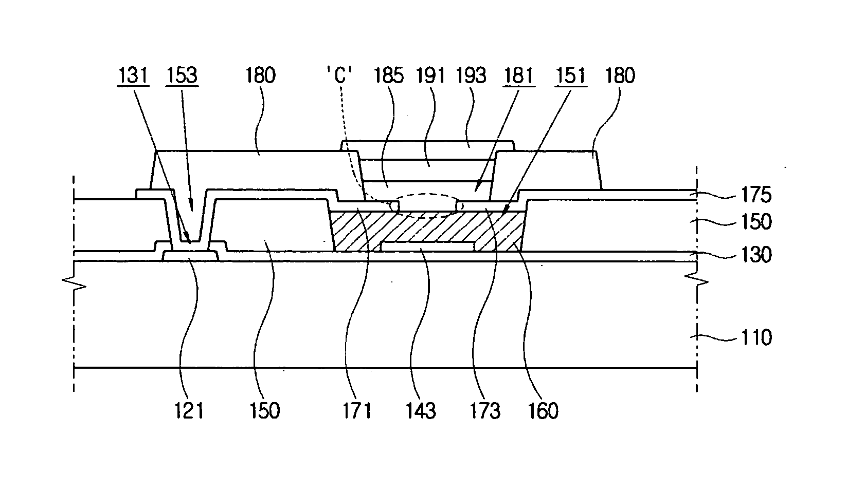
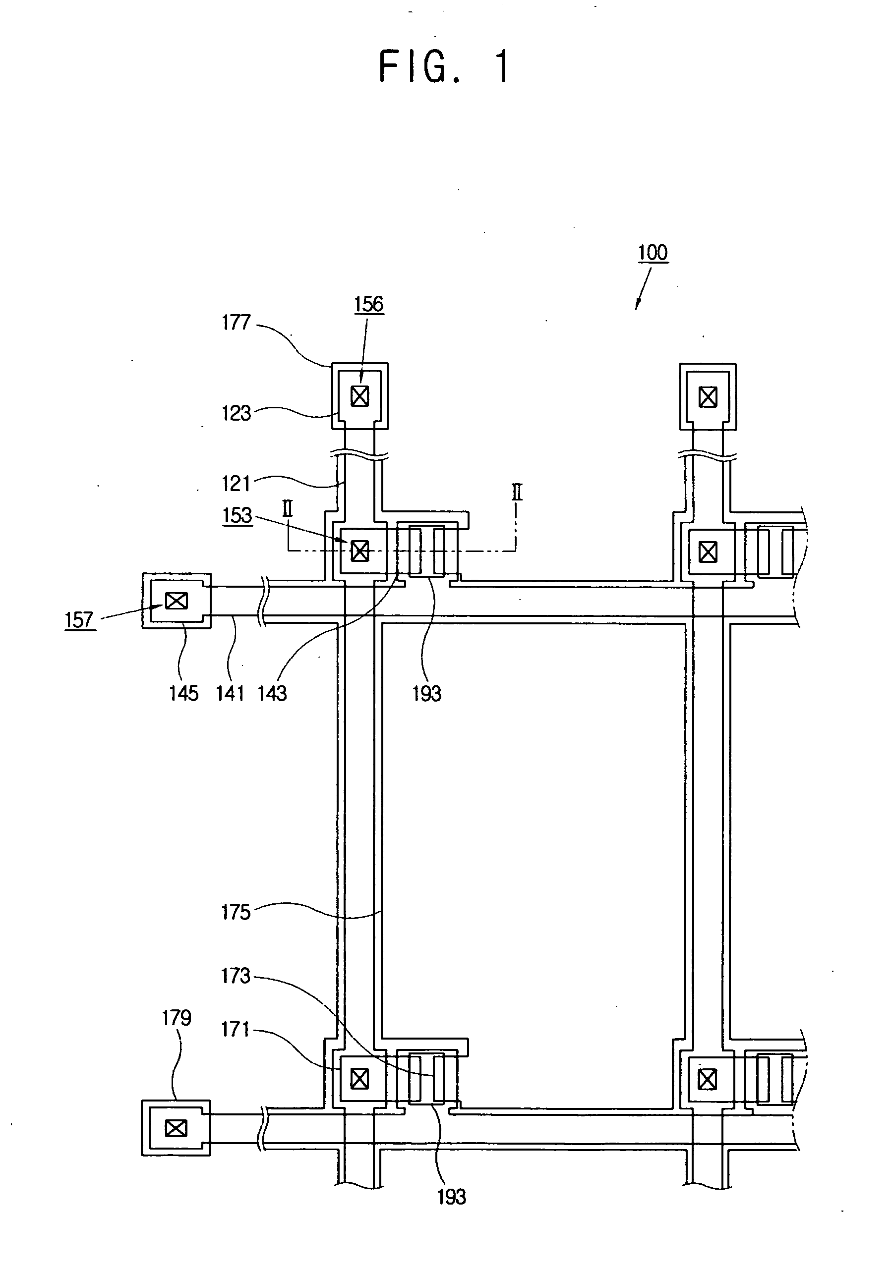
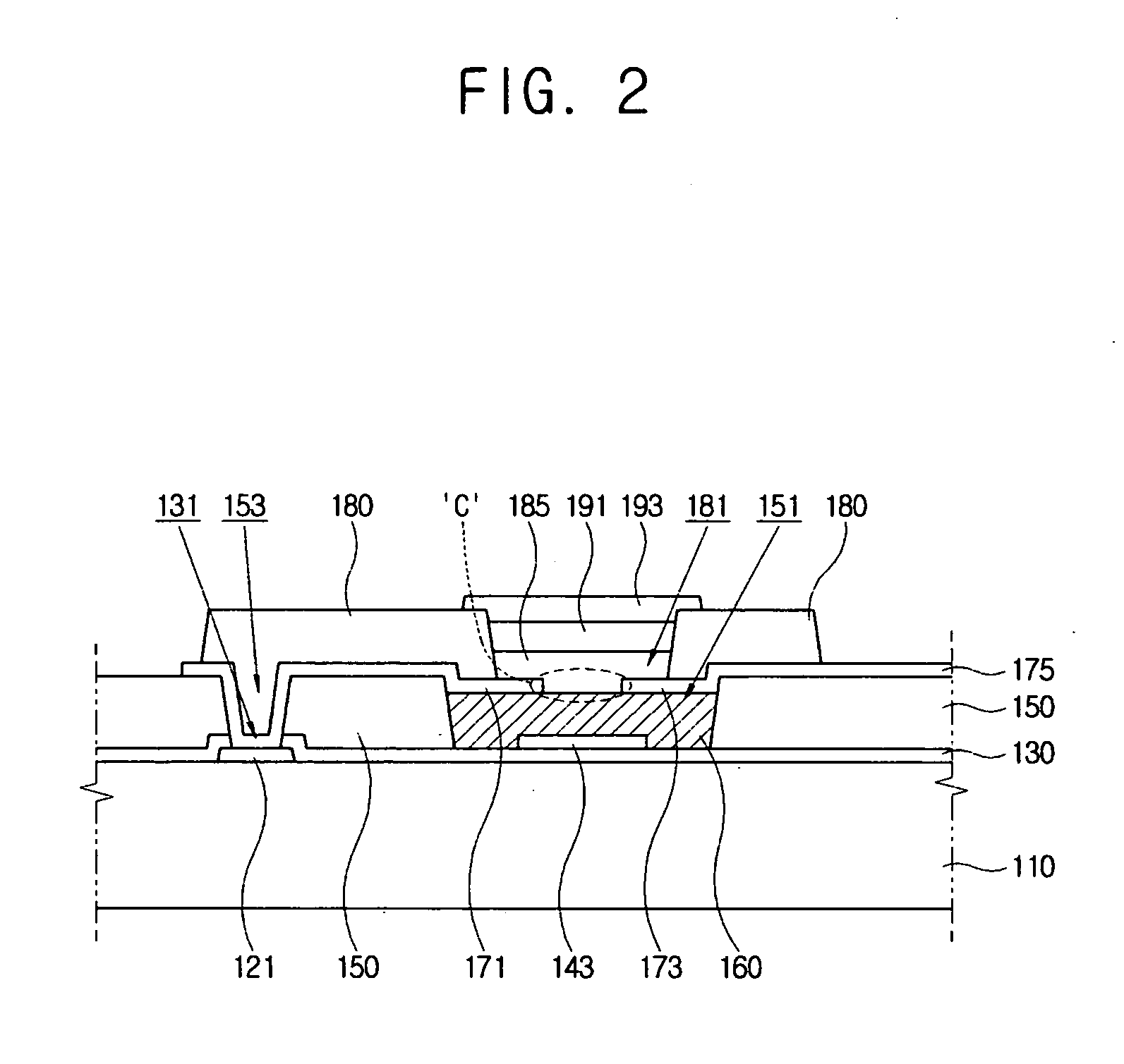
[0030]FIG. 1 illustrates a layout view of a thin film transistor (TFT) substrate according to the present invention, and FIG. 2 shows a cross-sectional view taken along line II-II in FIG. 1. The TFT substrate 100 according to an embodiment of the present invention comprises an insulating substrate 110; data wires 121 and 123 formed on the insulating substrate 110; an interlayer insulating film 130 formed on the data wires 121 and 123; gate wires 141, 143 and 145 formed on the interlayer insulating film 130; a second barrier wall 150 having a second opening 151 for exposing at least a portion of the gate wires 141, 143 and 145, and a barrier wall contact hole 153; a gate insulating film 160 formed inside the second opening 151; electrode layers 171, 173, 175, 177 and 179 including source and drain electrodes 171 and 173 which are spaced apart from each other with a gate electrode 143 disposed therebetween to define a channel region ‘C’; a first barrier wall 180 having a first opening...

second embodiment

[0061] because the gate insulating film 160 is covered by the electrode material layer 170, plasma, a chemical substance or the like used in the surface treatment can not flow into the gate insulating film 160. Therefore, a property of the gate insulating film 160 is not changed, and an organic semiconductor solution is uniformly spread on the channel region ‘C’ so that a characteristic of an O-TFT is enhanced.

[0062] Thereafter, a source electrode 171, a drain electrode 173, a pixel electrode 175, a data pad contact member (not shown) and a gate pad contact member (not shown) are formed by patterning the electrode material layer 170 as shown in FIG. 4G. The formation of the electrode layers 171, 173, 175, 177 and 179 comprises the operations of: forming a photosensitive film on the first barrier wall 180 and the electrode material layer 170; positioning and light-exposing a mask with an aperture of a predetermined pattern on the photosensitive film; developing the photosensitive fi...


PUM


Abstract

According to an embodiment of the present invention, a manufacturing method of a display device includes forming a plurality of gate wires comprising a gate electrode on an insulating substrate, forming an electrode layer comprising a source electrode and a drain electrode spaced apart from each other to define a channel region on the gate electrode interposed therebetween, forming a first barrier wall having a first opening for exposing the channel region, a portion of the source electrode, and a portion of the drain electrode on the electrode layer where the first barrier wall has a surface, forming a shielding film to cover the channel region inside the first opening, treating the surface of the first barrier wall, removing the shielding film, and forming an organic semiconductor layer inside the first opening.

Description

CROSS-REFERENCE TO RELATED APPLICATION [0001] This application claims priority to Patent Application No. 2005-0111023, filed on Nov. 19, 2005, in the Korean Intellectual Property Office, Republic of Korea, the entire content of which is hereby incorporated by reference. BACKGROUND [0002] (a) Field of the Invention [0003] The present invention relates to a display device and a manufacturing method thereof, and more particularly, to a display device including an organic thin film transistor (OTFT) and a manufacturing method thereof. [0004] (b) Description of Related Art [0005] Among various display devices, the flat display device with its small and lightweight characteristics has recently become more prominent. A liquid crystal display (LCD), such as an organic light emitting diode (OLED) device or the like, is used as such a flat display device and includes at least one thin film transistor to realize an image. The thin film transistor (TFT), which is a switching or driving device f...

Claims


Application Information

Patent Timeline
IPC IPC(8): H01L51/00H01L51/40
CPCB82Y30/00H01L27/3244H01L51/0005H01L51/0016H01L51/0545H01L51/0558H10K71/135H10K71/221H10K59/12H10K10/484H10K10/466G02F1/136
Inventor OH, JOON-HAKHONG, MUN-PYOKIM, BO-SUNGLEE, YONG-UK
Owner SAMSUNG DISPLAY CO LTD
Features
  • R&D
  • Intellectual Property
  • Life Sciences
  • Materials
  • Tech Scout
  • Unparalleled Data Quality
  • Higher Quality Content
  • 60% Fewer Hallucinations
Learn More