Integrated circuit stacking system with integrated passive components

a technology of integrated circuits and passive components, applied in the direction of semiconductor devices, semiconductor/solid-state device details, inductances, etc., can solve the problems of increasing cost, reducing the efficiency of integrated circuits, and large size of analog circuit components,

Active Publication Date: 2007-05-24
JCET SEMICON (SHAOXING) CO LTD
View PDF24 Cites 61 Cited by
  • Summary
  • Abstract
  • Description
  • Claims
  • Application Information

AI Technical Summary

Benefits of technology

[0011] The present invention provides an integrated circuit stacking system including fabricating an integrated passive device including: providing a semiconductor substrate, forming an integrated inductor, a resistor block, or an integrated capacitor integrated on the semiconductor substrate, and forming contact pads, on the semiconductor substrate, coupled to the integrated inductor, the resistor block, or the integrated capacitor; positioning an integrated circuit die for maintaining an inductor spacing; mounting the integrated circuit die on the integrated passive device; and encapsulating the integrated circuit die and the integrated passive device.

Problems solved by technology

One of the major challenges in the creation of analog processing circuitry (using digital processing procedures and equipment) is that a number of the components that are used for analog circuitry are large in size and are therefore not readily integrated into integrated circuits.
The main components that offer a challenge in this respect are capacitors and inductors, since both these components are, for typical analog processing circuits, of considerable size.
The conventional gold wire bonding technologies are facing challenges with bare copper pads because pad oxidation inhibits a mature bonding process.
In order to satisfy the demand for these necessary components, semiconductor technologies have added additional layers and special processing that increase cost and reduce the overall yield.
Solutions to these problems have been long sought but prior developments have not taught or suggested any solutions and, thus, solutions to these problems have long eluded those skilled in the art.

Method used


Image

  • Integrated circuit stacking system with integrated passive components
  • Integrated circuit stacking system with integrated passive components
  • Integrated circuit stacking system with integrated passive components

Examples


Embodiment Construction

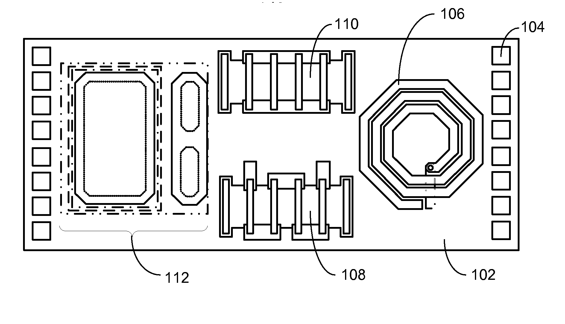
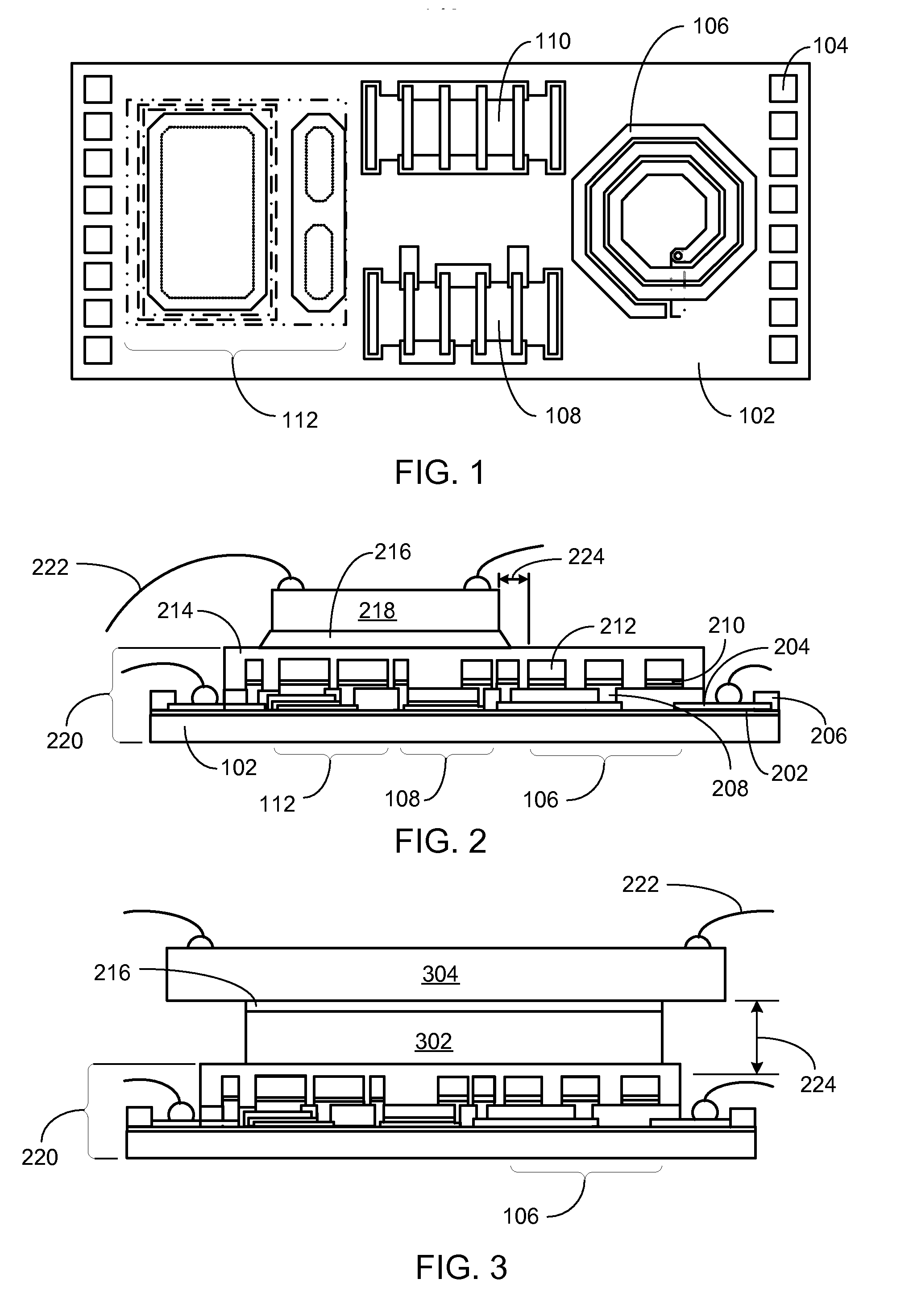
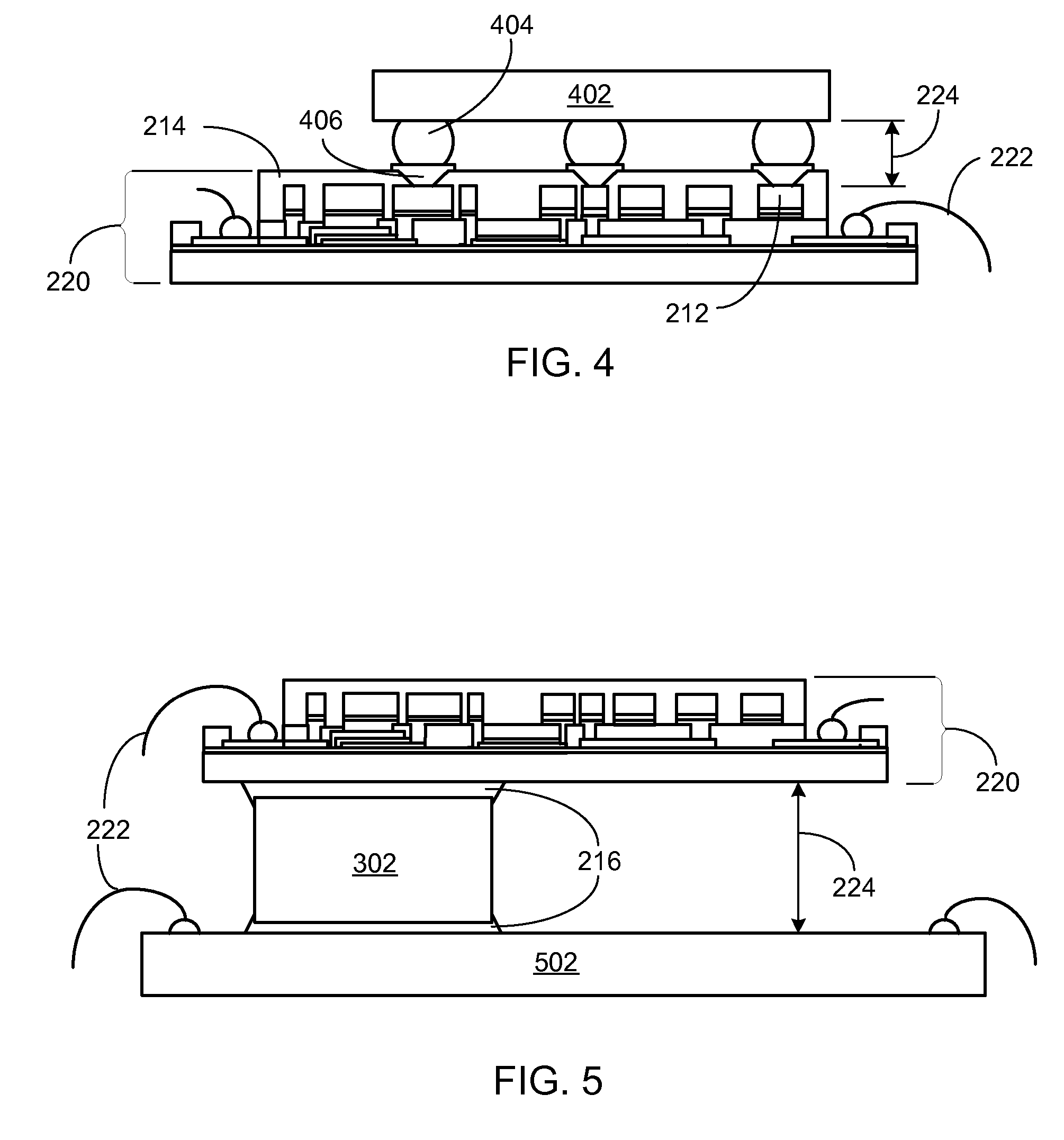
[0027] The following embodiments are described in sufficient detail to enable those skilled in the art to make and use the invention. It is to be understood that other embodiments would be evident based on the present disclosure, and that process or mechanical changes may be made without departing from the scope of the present invention.

[0028] In the following description, numerous specific details are given to provide a thorough understanding of the invention. However, it will be apparent that the invention may be practiced without these specific details. In order to avoid obscuring the present invention, some well-known circuits, system configurations, and process steps are not disclosed in detail. Likewise, the drawings showing embodiments of the system are semi-diagrammatic and not to scale and, particularly, some of the dimensions are for the clarity of presentation and are shown greatly exaggerated in the drawing FIGS. Where multiple embodiments are disclosed and described, h...


PUM


Abstract

An integrated circuit stacking system is provided including fabricating an integrated passive device including: providing a semiconductor substrate, forming an integrated inductor, a resistor block, or an integrated capacitor integrated on the semiconductor substrate, and forming contact pads, on the semiconductor substrate, coupled to the integrated inductor, the resistor block, or the integrated capacitor; positioning an integrated circuit die for maintaining an inductor spacing; mounting the integrated circuit die on the integrated passive device; and encapsulating the integrated circuit die and the integrated passive device.

Description

CROSS-REFERENCE TO RELATED APPLICATION(S) [0001] This application claims the benefit of U.S. Provisional Patent Application Ser. No. 60 / 596,925 filed Oct. 29, 2005.[0002] The present application contains subject matter related to co-pending U.S. patent application Ser. No. 11 / 278,002 by Yaojian Lin and Pandi Chelvam Marimuthu entitled “Integrated Circuit Package System with Post-Passivation Interconnection and Integration”. The related application is assigned to STATS ChipPAC Ltd. TECHNICAL FIELD [0003] The present invention relates generally to integrated circuits and more particularly to integrated circuit packaging. BACKGROUND ART [0004] Modern consumer electronics, such as smart phones, personal digital assistants, and location based services devices, as well as enterprise electronics, such as servers and storage arrays, are packing more integrated circuits into an ever shrinking physical space with expectations for decreasing cost. Every new generation of integrated circuits wi...

Claims


Application Information

Patent Timeline
Patent Type & Authority Applications(United States)
IPC IPC(8): H01L23/48H01L23/34
CPCH01F2017/0046H01L23/645H01L24/85H01L2224/16H01L2224/48091H01L2224/48463H01L2224/73265H01L2924/01013H01L2924/01029H01L2924/01079H01L2924/14H01L2924/19011H01L2924/19041H01L2924/19051H01L2924/19105H01L2924/00014H01L24/83H01L2224/85H01L24/48H01L2924/01019H01L2224/45144H01L2924/00H01L2224/83H01L2924/15787H01L2924/181H01L24/45H01L2924/00015
Inventor MARIMUTHU, PANDI CHELVAMFRYE, ROBERT CHARLESLIN, YAOJIAN
Owner JCET SEMICON (SHAOXING) CO LTD
Why Eureka
Try Eureka