Method for manufacturing liquid crystal display device

a liquid crystal display and liquid crystal technology, applied in the field of liquid crystal display devices, can solve the problems of static electricity generation and dust generation, destruction of a switching element formed over a substrate, and difficulty in uniform irradiation of light energy with respect to a substrate surface, etc., to achieve high contrast, wide viewing angle, and high quality black display

Active Publication Date: 2007-05-24
SEMICON ENERGY LAB CO LTD
View PDF10 Cites 13 Cited by
  • Summary
  • Abstract
  • Description
  • Claims
  • Application Information

AI Technical Summary

Benefits of technology

[0029] The liquid crystal display device of the present invention employs a driving method in which VA (Vertically Aligned) mode liquid crystal with a negative dielectric anisotropy is aligned vertically in a no-voltage state and aligned horizontally in a state with a voltage applied. Since liquid crystal is aligned in a vertical direction in a no-voltage state, the liquid crystal display device has advantages of high-quality black display, high contrast, wide viewing angle, and high-speed response.
[0030] Since the present invention does not require rubbing treatment and optical alignment treatment, liquid crystal molecules can be uniformly aligned even in a large-screen liquid crystal display device using a large-area substrate.

Problems solved by technology

However, since rubbing is a method of directly rubbing an alignment film with cloth, it has problems of static electricity generation and dust generation by scraping the alignment film.
The static electricity generation may result in destruction of a switching element formed over a substrate.
Therefore, it is difficult to uniform irradiation light energy with respect to a surface of a substrate, and a pretilt angle may become uneven.

Method used


Image

  • Method for manufacturing liquid crystal display device
  • Method for manufacturing liquid crystal display device
  • Method for manufacturing liquid crystal display device

Examples


experiment 1

(Experiment 1)

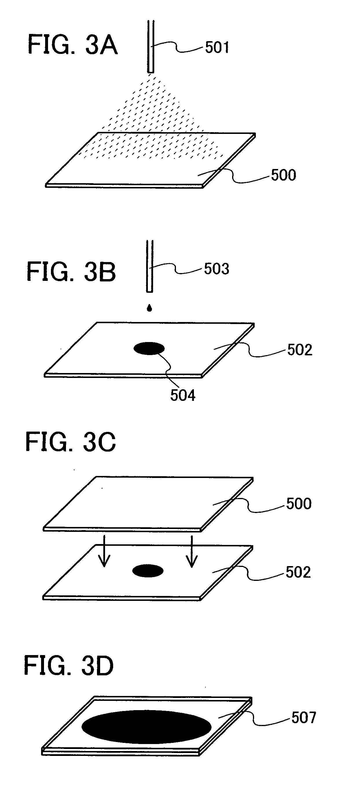
[0060]FIGS. 3A to 3D show a manufacturing process for an evaluation liquid crystal element. First, a spherical spacer (a bead spacer with a diameter of 1.9 μm) was sprayed using a spray nozzle 501 over a first substrate 500 which was provided with a transparent electrode (ITO) as shown in FIG. 3A. Next, a mixture 504 of VA mode liquid crystal (MLC 2038) in which octadecyltrimethoxysilane (hereinafter referred to as ODS) of 10 wt % was dispersed was dropped from a dropping nozzle 503 to a surface of a second substrate 502 which was provided with a transparent electrode (ITO), as shown FIG. 3B. Then, the first substrate and the second substrate were attached to each other as shown in FIG. 3C. At that time, a gap between the pair of substrates was maintained with the spherical spacer. A liquid crystal element 507 manufactured as described above and shown in FIG. 3D was an evaluation element. The structure of the evaluation liquid crystal element manufactured as described ...

embodiment mode 2

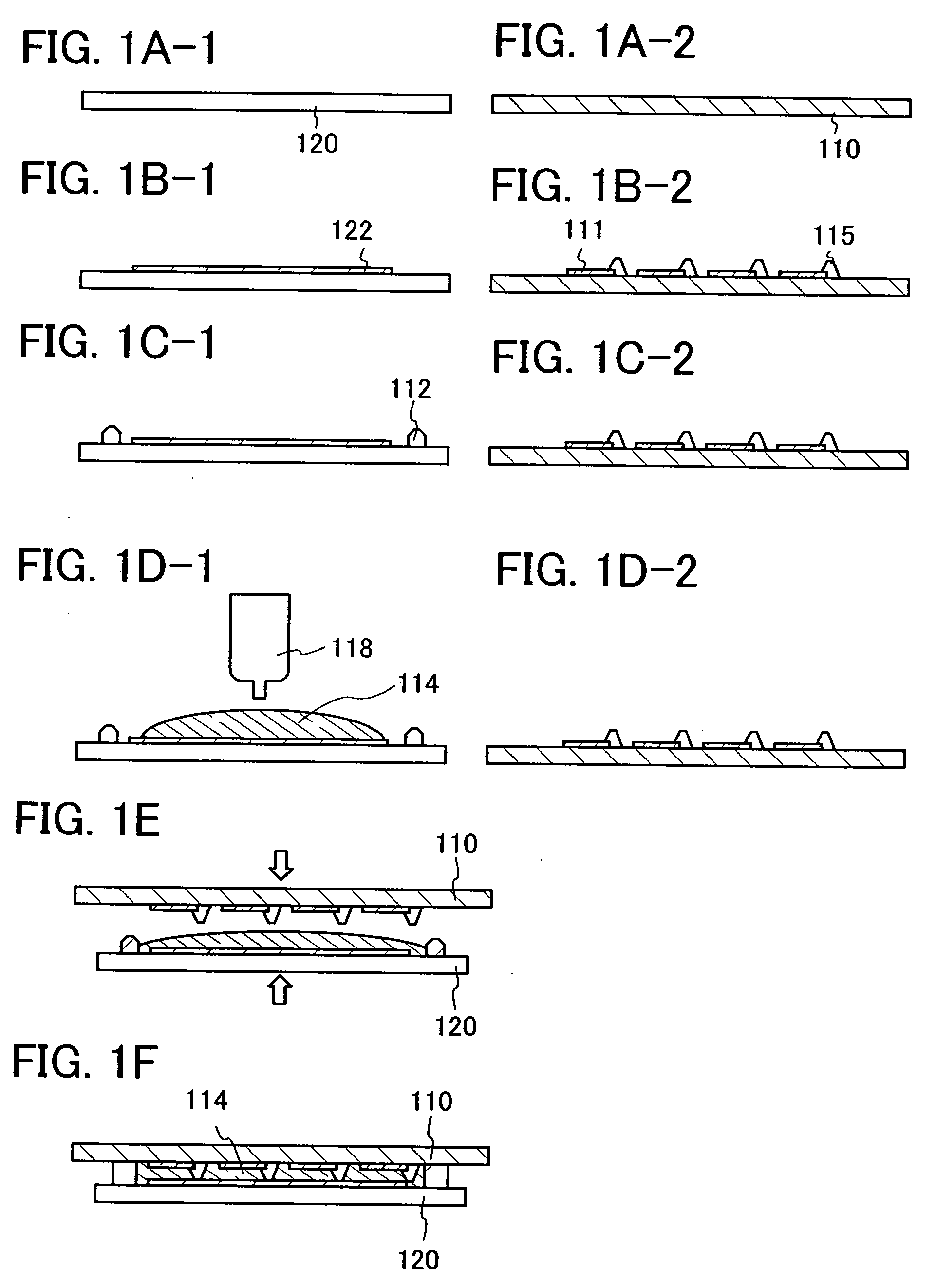
[0063] Here, explained is an example of performing seal drawing on a first substrate side and injecting liquid crystal after attaching a pair of substrates to each other. The flow of panel manufacturing is explained below.

[0064] First, a second substrate 220 serving as an opposite substrate and a first substrate 210 provided with TFTs (not shown) in advance are prepared as shown in FIG. 5A-1 and FIG. 5A-2. Note that an opposite electrode 222 made of a transparent conductive film is formed over the second substrate 220, and a pixel electrode 211 made of a transparent conductive film is formed over the first substrate 210 in advance.

[0065] Next, a spherical spacer 215 is sprayed over the second substrate 220, and a sealant 212 is drawn over the first substrate 210 as shown in FIG. 5B-1 and FIG. 5B-2. Although the sealant 212 is arranged so as to surround a display region, the sealant 212 is not arranged in a portion later serving as an inlet (not shown here) for injecting liquid cry...

experiment 2

(Experiment 2)

[0075] A pair of substrates each provided with a transparent electrode (ITO) was attached to each other using a thermosetting seal. In addition, a bead spacer with a diameter of 1.9 μm was dispersed in the seal to maintain a distance between the substrates, which was used as an evaluation element.

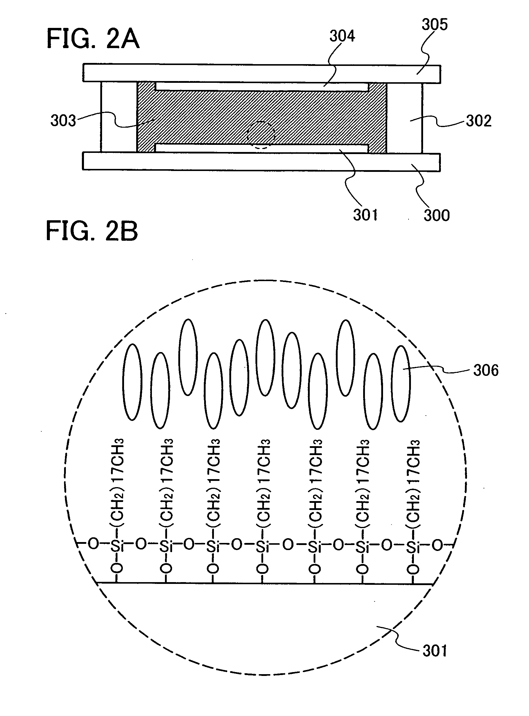
[0076] After that, liquid crystal in which ODS of 0 wt % to 10 wt % was dispersed was injected between the pair of substrates and heated at 130° C. for one hour, thereby performing realignment treatment. ODS dispersed in liquid crystal adsorbs to an interface of ITO or a substrate after the injection and forms a self-assembled monolayer. The structure of the evaluation liquid crystal element manufactured as described above is similar to that in FIGS. 2A and 2B.

[0077] The evaluation liquid crystal element manufactured as described above was evaluated under similar conditions to those of Experiment 1 by the system of measurement shown in FIG. 4. A result of transmitted light l...


PUM

PropertyMeasurementUnit
sizeaaaaaaaaaa
sizeaaaaaaaaaa
sizeaaaaaaaaaa

Abstract

An object is to uniformly align liquid crystal molecules without requiring a step of forming an alignment film. A material for forming a self-assembled monolayer is dispersed in a liquid crystal material, and the mixture is interposed between a pair of substrates by a liquid crystal injection method or a liquid crystal dropping method. A silane coupling agent (the material for forming a self-assembled monolayer) injected or dropped with the liquid crystal material adsorbs to a substrate interface (or a surface of an electrode formed over a substrate) after the injection or dropping, thereby forming a self-assembled monolayer. This self-assembled monolayer serves as an alignment film, and enables long axes of liquid crystal molecules to be approximately perpendicular to a substrate and the liquid crystal molecules to be uniformly aligned.

Description

TECHNICAL FIELD [0001] The present invention relates to a liquid crystal display device and a method for manufacturing the liquid crystal display device. The present invention relates to, for example, an electro-optical device typified by a liquid crystal display panel which has a circuit including a thin film transistor (hereinafter referred to as a TFT), and an electronic device equipped with such an electro-optical device as a component. BACKGROUND ART [0002] In recent years, a technique for forming a thin film transistor (TFT) using a semiconductor thin film (with a thickness of approximately several to several hundreds nm) which is formed over a substrate having an insulating surface has attracted attention. The thin film transistor is widely applied to an electronic device such as an electro-optical device or an IC, and has been hurriedly developed particularly as a switching element of a liquid crystal display device. [0003] In a liquid crystal display device used for a noteb...

Claims


Application Information

Patent Timeline
Patent Type & Authority Applications(United States)
IPC IPC(8): C09K19/52C09K19/54C09K19/00
CPCB82Y30/00G02F1/1341Y10T428/10Y10T428/1036Y10T428/1059G02F2001/13415C09K2323/05C09K2323/03C09K2323/00G02F1/13415G02F1/1339C09K19/00
Inventor KUBOTA, DAISUKENISHI, TAKESHIYAMASHITA, AKIO
Owner SEMICON ENERGY LAB CO LTD
Why Eureka
Try Eureka