Via array capacitor, wiring board incorporating a via array capacitor, and method of manufacturing the same

a technology of array capacitors and wiring boards, which is applied in the direction of stacked capacitors, fixed capacitors, fixed capacitor details, etc., can solve the problems of affecting the reliability of the wiring board, the likelihood of fracture or breakage of the array capacitor, and the crack formation of the array capacitor. , to achieve the effect of improving strength, preventing breakage, and improving flexibility

Inactive Publication Date: 2007-05-24
NGK SPARK PLUG CO LTD
View PDF4 Cites 62 Cited by
  • Summary
  • Abstract
  • Description
  • Claims
  • Application Information

AI Technical Summary

Benefits of technology

[0005] The invention has been devised in view of the above-described problems, and its object is to provide a via array capacitor which, even if the thickness is made thin, is able to prevent breakage by improving its flexibility. Another object of the invention is to provide a wiring board incorporating a via array capacitor capable of attaining improvement of the low height and reliability by incorporating the aforementioned via array capacitor, as well as a method of manufacturing the same.
[0040] Therefore, according to the wiring board incorporating a via array capacitor in accordance with the sixth aspect, by setting the total thickness of the metal-containing layers or the reinforced metal layer (s) to not less than 15% and not more than 80% of the overall thickness of the via array capacitor, or by setting the total volume of the inner electrode layers and the metal-containing layers to not less than 45 vol. % and not more than 95 vol. % of the aggregate volume of the entire via array capacitor, the proportion of the metal portions becomes high for the via array capacitor as a whole. As a result, the overall via array capacitor is reinforced by the metal portions, the flexibility improves, and its own strength improves, so that it is possible to prevent the breakage of the via array capacitor even in cases where the overall thickness of the via array capacitor is made thin. Therefore, as such a via array capacitor is incorporated, it is possible to attain improvement of the low height and reliability of the wiring board incorporating a via array capacitor. Also, it is possible to prevent a decline in capacitance due to breakage.

Problems solved by technology

This via array capacitor is likely to be fractured or broken during handling since its thickness is thin although it has a larger area than a chip type capacitor.
In addition, a problem can possibly occur in that a crack is formed in the via array capacitor in the step of its incorporation into the buildup layer.
Further, even if a crack does not occur in the incorporating step, the reliability of the wiring board can also possibly decline due to the incorporation of the via array capacitor having a thin thickness although it has a larger area than the chip type capacitor.

Method used


Image

  • Via array capacitor, wiring board incorporating a via array capacitor, and method of manufacturing the same
  • Via array capacitor, wiring board incorporating a via array capacitor, and method of manufacturing the same
  • Via array capacitor, wiring board incorporating a via array capacitor, and method of manufacturing the same

Examples


Embodiment Construction

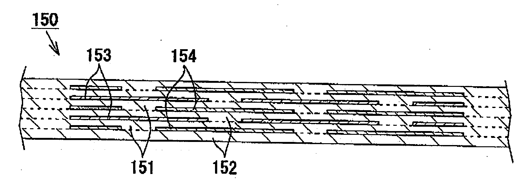
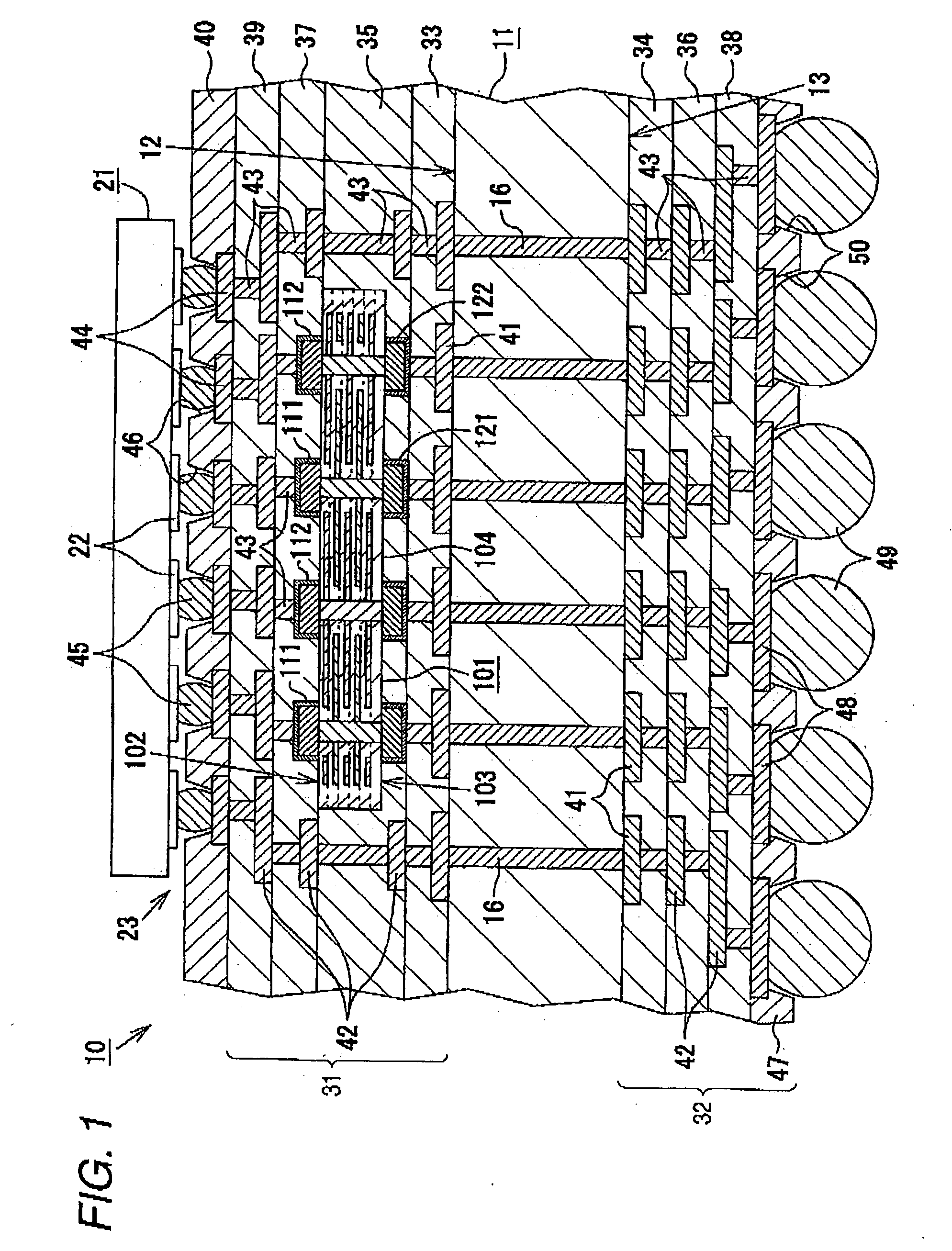
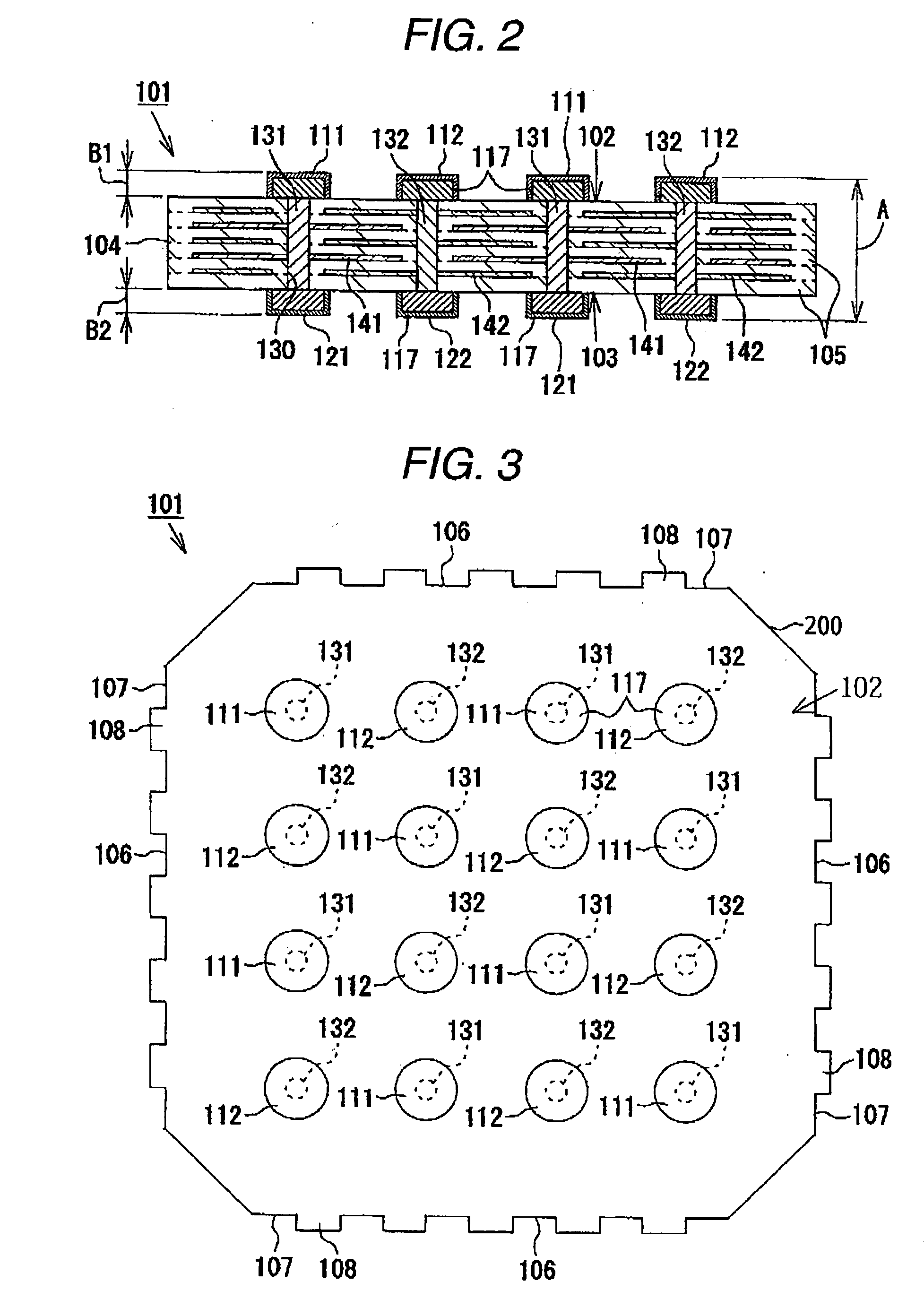
[0093] Referring now to the accompanying drawings, a detailed description will be given of an embodiment of a wiring board incorporating a via array capacitor in accordance with the invention.

[0094] As shown in FIG. 1, a wiring board 10 incorporating a via array capacitor in accordance with this embodiment is a wiring board for mounting on an IC chip, and is comprised of a substantially rectangular plate-shaped core board 11 which is formed of glass epoxy; a build up layer 31 (laminated portion) formed on an upper surface 12 of the core board 11; and a buildup layer 32 formed on a lower surface 13 of the core board 11. Via conductors 16 are formed at a plurality of portions in the core board 11. These via conductors 16 connect and conduct the upper surface 12 side and the lower surface 13 side of the core board 11. Further, conductor layers 41 formed of copper are respectively pattern-formed on the upper surface 12 and the lower surface 13 of the core board 11, and each conductor l...


PUM


Abstract

A via array capacitor comprising: a capacitor body including a first main surface and a second main surface and having a structure in which dielectric layers and inner electrode layers are alternately laminated; a plurality of via conductors which conduct the inner electrode layers to each other and are, as a whole, arranged in array form; and metal-containing layers which are disposed on at least one of the first main surface and the second main surface, wherein a total of a thickness of the metal-containing layers disposed on the first main surface and a thickness of the metal-containing layers disposed on the second main surface is from 15% to 80% of an overall thickness of the via array capacitor.

Description

FIELD OF THE INVENTION [0001] The present invention relates to a via array capacitor which is incorporated in a laminated portion of a wiring board, a wiring board incorporating a via array capacitor having a via array capacitor, and a method of manufacturing the same. BACKGROUND OF THE INVENTION [0002] Semiconductor devices (IC chips) used in CPUs of computers in recent years tend to be characterized by increasingly higher speed and higher functions, and the number of terminals tends to increase and the pitch between the terminals tends to become narrower correspondingly. Generally, a multiplicity of terminals are densely arranged in array form on the bottom surface of the IC chip, and such terminal groups are connected to terminal groups on the motherboard side in flip chip form. However, since there is a large difference in the terminal pitch between the terminal groups on the IC chip side and the terminal groups on the motherboard side, it is difficult to directly connect the IC...

Claims


Application Information

Patent Timeline
Patent Type & Authority Applications(United States)
IPC IPC(8): H01L21/20H01L29/00
CPCH01G4/232H01L2224/16235H01L23/49822H01L23/50H01L24/81H01L2224/16H01L2224/81192H01L2224/81801H01L2224/82039H01L2224/82047H01L2924/01078H01L2924/09701H01L2924/15174H01L2924/15311H05K1/0231H05K1/112H05K1/186H05K3/4602H05K2201/10674H05K2201/10712H01L2924/01019H01G4/30H01L2224/05568H01L2224/05573H01L2924/14H01L2924/3511H01L2924/00
Inventor YAMAMOTO, HIROSHISEKI, TOSHITAKEOTSUKA, JUNSATO, MANABUOKUYAMA, MASAHIKO
Owner NGK SPARK PLUG CO LTD
Why Eureka
Try Eureka