Process and equipment for bonding by molecular adhesion

a technology of molecular adhesion and equipment, applied in the direction of packaging, transportation and packaging, paper/cardboard containers, etc., can solve the problems of edge type defects, no component can be manufactured, edge type defects, etc., to improve the bonding speed, facilitate bonding, and correct the disadvantages of the state of the art

Active Publication Date: 2007-05-31
S O I TEC SILICON ON INSULATOR THECHNOLOGIES
View PDF9 Cites 48 Cited by
  • Summary
  • Abstract
  • Description
  • Claims
  • Application Information

AI Technical Summary

Benefits of technology

[0029] The present invention provides bonding techniques that rectify the disadvantages of the state of the art. The invention generally relates to a method for bonding two substrates together by molecular adhesion of their surfaces which comprises preparing the surfaces of the substrates with a flatness sufficient to facilitate bonding by propagation of a bonding front when the surfaces of the substrates are placed in contact with each other, modifying the surface of one or both of the substrates sufficiently to regulate propagation speed of the bonding front to reduce bubble or voids between the substrates after bonding. Enhanced bonding can be achieved by modifying the surface(s) to decrease water adsorbed thereon. Thereafter, the surfaces of the substrates can be placed in contact together to effect bonding with the modified surface(s) providing a sufficiently reduced speed of the bonding from to reduce the number of bubbles or void defects therebetween compared to bonding with non-modified substrate surfaces.

Problems solved by technology

Also, bonding by molecular adhesion of substrates to one another generally causes defects.
Notable examples of such defects include defects of the bubble type (or bubbles) at the level of the bonding interface between the two substrates, as well as defects of edge type (or edge voids) at the level of the thin layer of the final structure (the thin layer on support substrate that is obtained after transfer).
Despite the accepted use of these processes, defects of the edge voids type, cause by the bonding step, can often appear after transfer of the thin layer from the donor substrate to the support substrate.
They can be killer defects because, in the absence of a thin layer acting as an active layer for the formation of electronic components at the location of an edge void, no component can be manufactured at this location.
Given the size of the edge voids, an electronic component comprising at least one edge void is necessarily defective.
This increased presence of edge voids tends to prohibit the recycling of such wafers, thus defeating one of the main reasons for using the SMART-CUT® process.
This solution thus has the disadvantage of requiring previous mechanical intervention on the wafers.
One solution for reducing the formation of bubbles in this process consists of producing plasma activation of the surfaces to be bonded, so as to obtain good adhesion energy, but this solution has not been found to be entirely satisfactory for reducing the number of bubbles at the bonding interface.

Method used


Image

  • Process and equipment for bonding by molecular adhesion
  • Process and equipment for bonding by molecular adhesion
  • Process and equipment for bonding by molecular adhesion

Examples


second embodiment

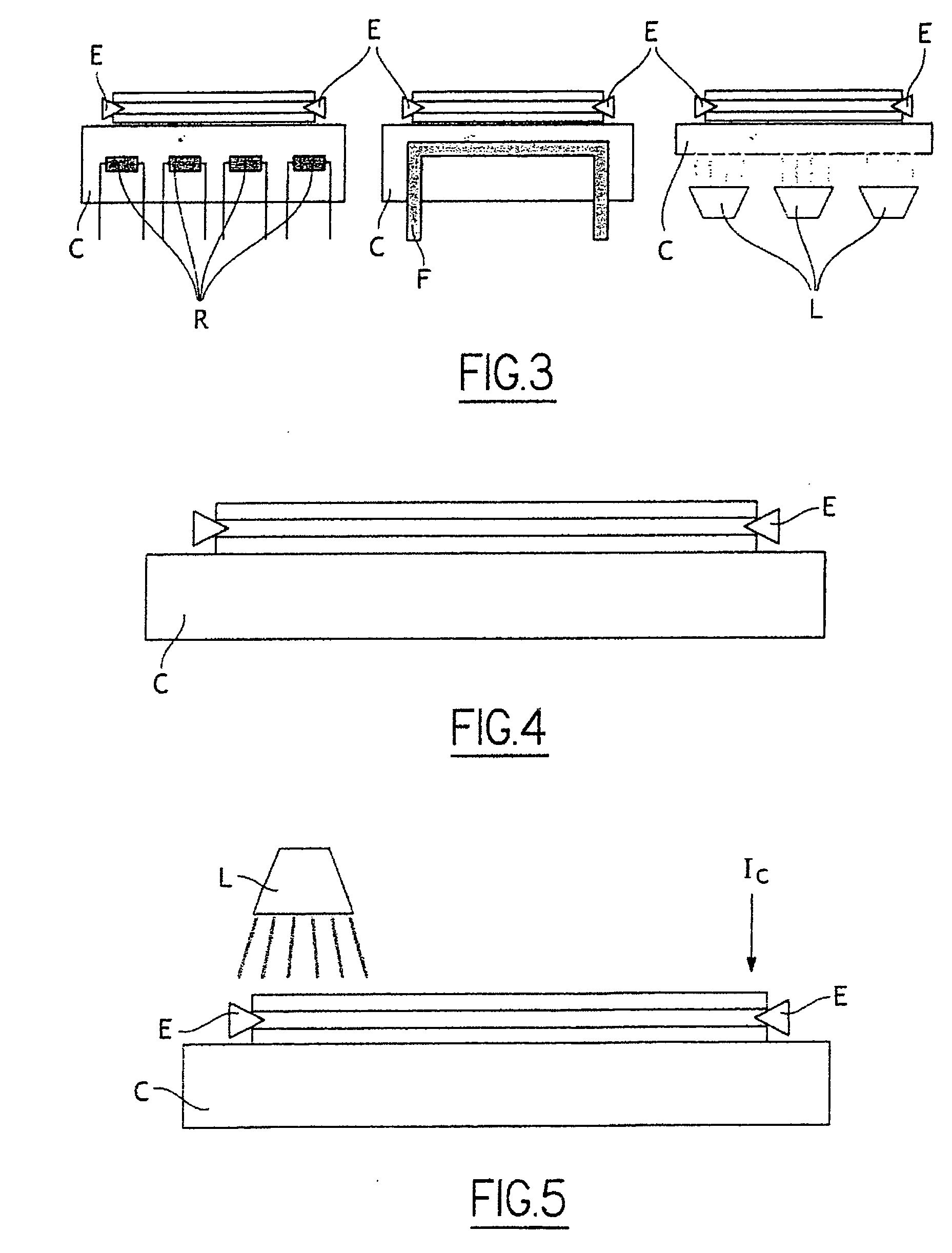
[0053] Rather than heating, additional techniques can be used to modify the surface(s) of the substrate to be bonded. Certain aspects, again preferred though non-limiting, of this second embodiment of this process are the following: [0054] modification of the surface state is effected by roughing the surface: [0055] the modification step of the surface state includes forming a rough surface layer on one or both of the substrates to be bonded; [0056] to form the rough layer, the process comprises a thermal oxidation operation of one or both of the substrates so as to form a thermal oxide layer thereon and an operation for treating the thermal oxide layer adapted to etch the oxide layer: [0057] treatment of the thermal oxide layer can be accomplished by other chemical treatments rather than etching; [0058] the layer of thermal oxide is a layer of SiO2 and the chemical treatment is SC1 treatment conducted at a temperature of between 50° C. and 80° C. over a period of longer than three ...

first embodiment

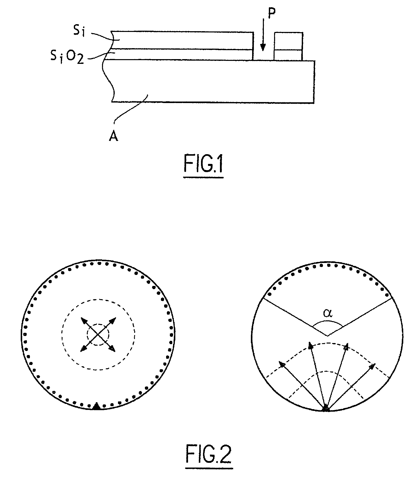
[0070] this means in particular to control the quantity of water adsorbed at the surface, and more precisely to decrease, without completely eliminating all the same, the thickness of the layer of water adsorbed relative to the thickness of the layer of water normally adsorbed. In other terms, this means to reduce the number of monolayers of water adsorbed at the surface. Bonding by molecular adhesion is also known as direct bonding, because it concerns bonding not requiring the application of an adhesive (of gum or other glue type). It is really the water adsorbed on each of the surfaces (several monolayers of water) and placed in contact which acts as adhesive and ensures adhesion by means of Van der Waals force. For this reason, it was previously considered that several monolayers of water must be present on the surface in order to obtain good molecular bonding.

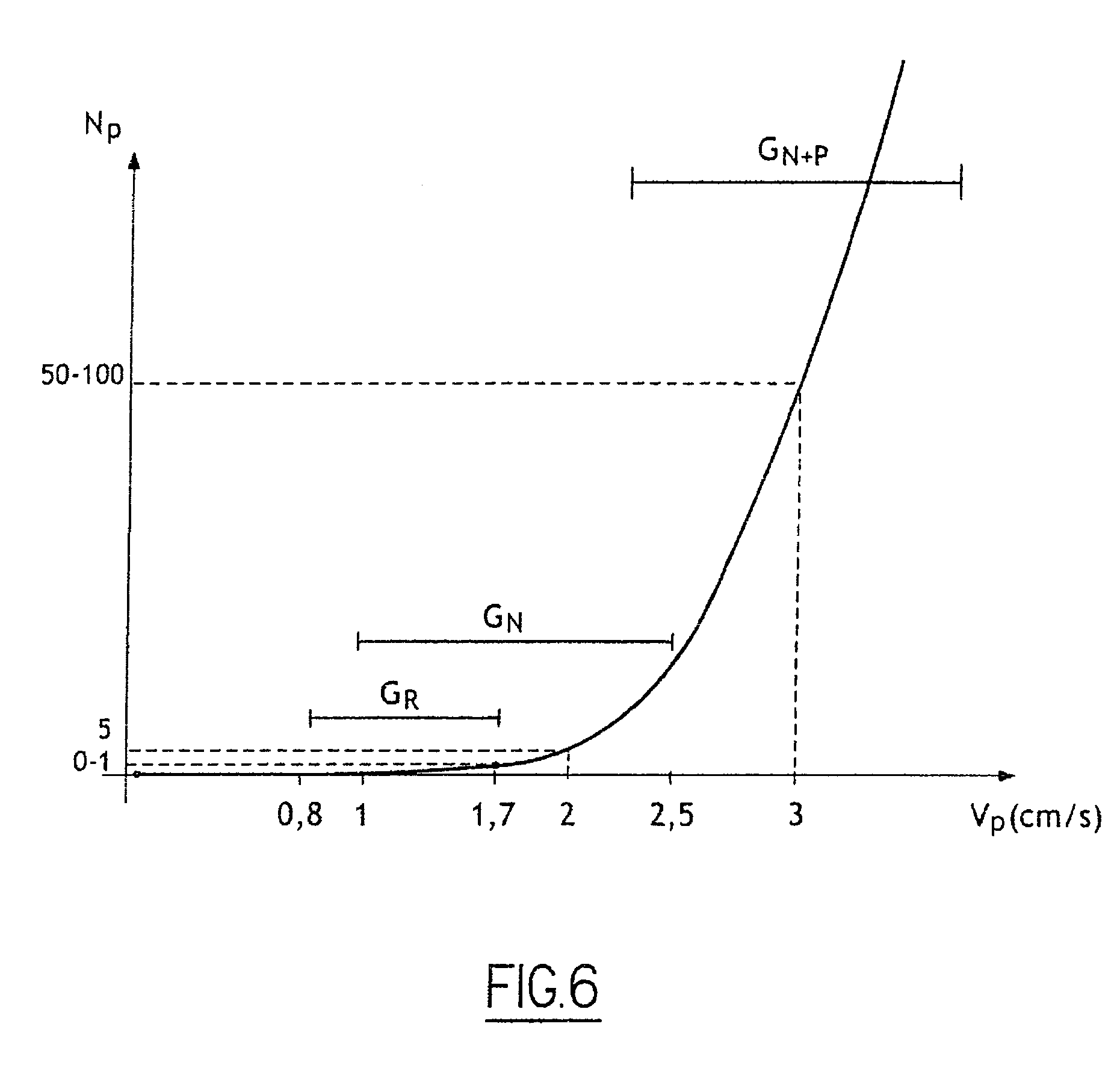
[0071] Within the scope of this first embodiment, the surface state of a substrate is modified, and the propagation spe...


PUM

PropertyMeasurementUnit
speedaaaaaaaaaa
speedaaaaaaaaaa
speedaaaaaaaaaa

Abstract

The invention relates to a process for bonding by molecular adhesion of two substrates to one another during which the surfaces of the substrates are placed in close contact and bonding occurs by propagation of a bonding front between the substrates. The invention includes, prior to bonding, a step of modifying the surface state of one or both of the surfaces of the substrates so as to regulate the propagation speed of the bonding front. The surface can be modified by locally or uniformly heating or roughening the surface(s) of the substrate(s).

Description

BACKGROUND [0001] The field of the invention is that of bonding two substrates to one another by molecular adhesion. The invention generally concerns a process and bonding equipment. It extends likewise to the formation of a structure comprising a thin layer made of a semiconductor material upon a support substrate. To form such a structure, the typical procedure is to place a donor substrate in close contact with the support substrate, so as to effect bonding by molecular adhesion of the substrates to one another. This is then followed by the transfer of a part of the donor substrate to the support substrate to form the thin layer on the support substrate. [0002] Bonding by molecular adhesion (either ‘direct wafer bonding’ or ‘fusion bonding’) is a technique that enables two substrates having perfectly flat surfaces (e.g., polished mirror surfaces) to adhere to one another, without the application of adhesive (gum type, glue, etc.). The surfaces in question are generally those of s...

Claims


Application Information

Patent Timeline
Patent Type & Authority Applications(United States)
IPC IPC(8): C03C15/00B31B1/60
CPCC03C27/00C03C27/02C03C27/046C03C2204/08H01L21/2007Y10T156/17H01L2924/1461H01L2224/75251Y10T156/10H01L2924/00H01L21/76251H01L2224/83002H01L21/20H01L21/762
Inventor KERDILES, SEBASTIENDURET, CARINEVAUFREDAZ, ALEXANDREMETRAL, FREDERIC
Owner S O I TEC SILICON ON INSULATOR THECHNOLOGIES
Why Eureka
Try Eureka