Circuit and method for suppression of electromagnetic coupling and switching noise in multilayer printed circuit boards
a multi-layer printed circuit board and electromagnetic coupling technology, applied in the incorporation of printed capacitors, waveguide type devices, line-transmission details, etc., can solve the problems of increasing material and manufacturing costs with increasing concomitantly, and achieve the effect of eliminating power plane resonance and suppressing digital nois
- Summary
- Abstract
- Description
- Claims
- Application Information
AI Technical Summary
Benefits of technology
Problems solved by technology
Method used
Image
Examples
first embodiment
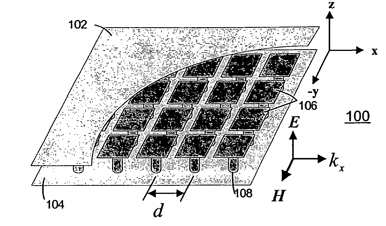
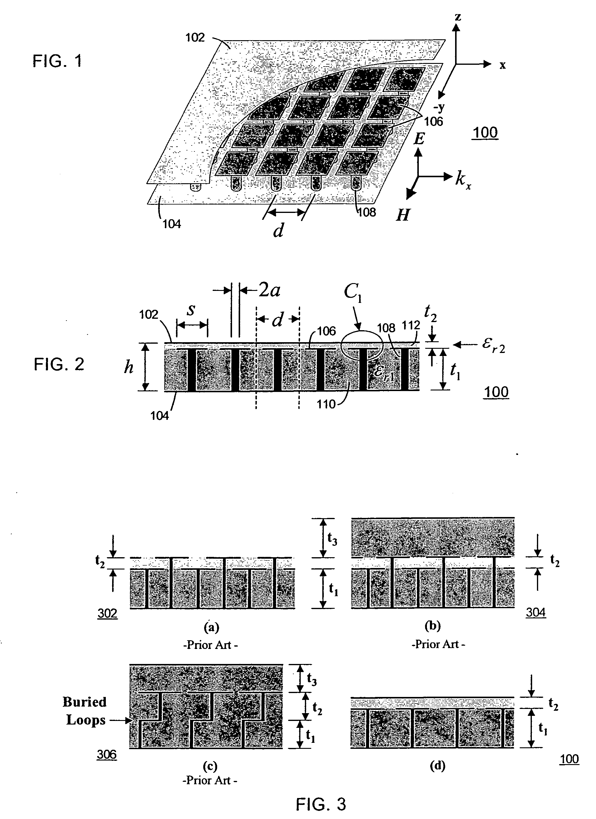
[0051] Referring now to the drawing, FIG. 1 and FIG. 2 illustrate a parallel plate wave guide (PPW) 100 containing a transverse electromagnetic (TEM) mode suppression circuit. FIG. 1 is a perspective view of the PPW 100 and FIG. 2 is a cross-sectional view of the PPW 100. Coordinate axes establish the x, y and z directions as used herein.
[0052] As shown in FIGS. 1 and 2, the PPW 100 includes an upper conductive plate 102, a lower conductive plate 104, an array of conductive coplanar patches 106 located a distance t2 from the upper plate 102, an array of conductive rods or vias 108 of length t1 and radius a that connect the lower plate 104 to the center of each patch 106, a first dielectric layer 110 and a second dielectric layer 112. The patches 106 are illustrated to be squares of side length s in FIG. 1, but other shapes such as rectangular, hexagonal, triangular, circular, etc. can be used. The patch realizes a parallel-plate capacitance between the end of the rod 108 below it an...
fourth embodiment
[0107] Yet another embodiment involves adding a spiral inductor in series with each via, as shown in FIGS. 16 and 17. The purpose of this added inductance is to reduce ƒlower. FIG. 16 and FIG. 17 illustrate a parallel plate waveguide (PPW) 1600. The PPW 1600 includes an upper conductive plate and a lower conductive plate (not shown in FIG. 16). The PPW 1600 includes an array of conductive coplanar patches 1606 located a distance t2 from the upper plate, an array of conductive rods or vias 1608 of length t1 and radius a that connect the lower plate to the center of each patch 1606, a first dielectric layer 1610 and a second dielectric layer 1612. The PPW 1600 further includes a spiral inductor 1612 associated with each respective patch 1606 and via 1608.
[0108] In the embodiment of FIGS. 16 and 17, the inductors 1614 and patches are coplanar and are etched as part of the same metal layer. The coplanar spiral inductor 1614 is formed within the perimeter of the patch 1606. The merit of ...
PUM
 Abstract
Description
Claims
Application Information


