Manufacturing method of display device and display device therefrom

a display device and manufacturing method technology, applied in the direction of discharge tube luminescnet screens, discharge tube/lamp details, electric discharge lamps, etc., can solve the problems of more complicated production process, increased power consumption with an increase in size and resolution, and uneven quality of organic layers

Active Publication Date: 2007-05-31
SAMSUNG DISPLAY CO LTD
View PDF4 Cites 10 Cited by
  • Summary
  • Abstract
  • Description
  • Claims
  • Application Information

AI Technical Summary

Benefits of technology

[0021] According to another aspect of the present invention, the ink and the second solvent are ejected through an inkjet method, and the second solvent is ejected less accurately than the ink.

Problems solved by technology

The passive matrix type has a simple production process, but drastically increases power consumption with an increase in size and resolution.
Meanwhile, the active matrix type realizes a wide screen and high resolution, but has a more complicated production process.
However, the quality of the organic layer is not uniform due to the varying drying conditions of ink according to ejected orders.

Method used


Image

  • Manufacturing method of display device and display device therefrom
  • Manufacturing method of display device and display device therefrom
  • Manufacturing method of display device and display device therefrom

Examples


Embodiment Construction

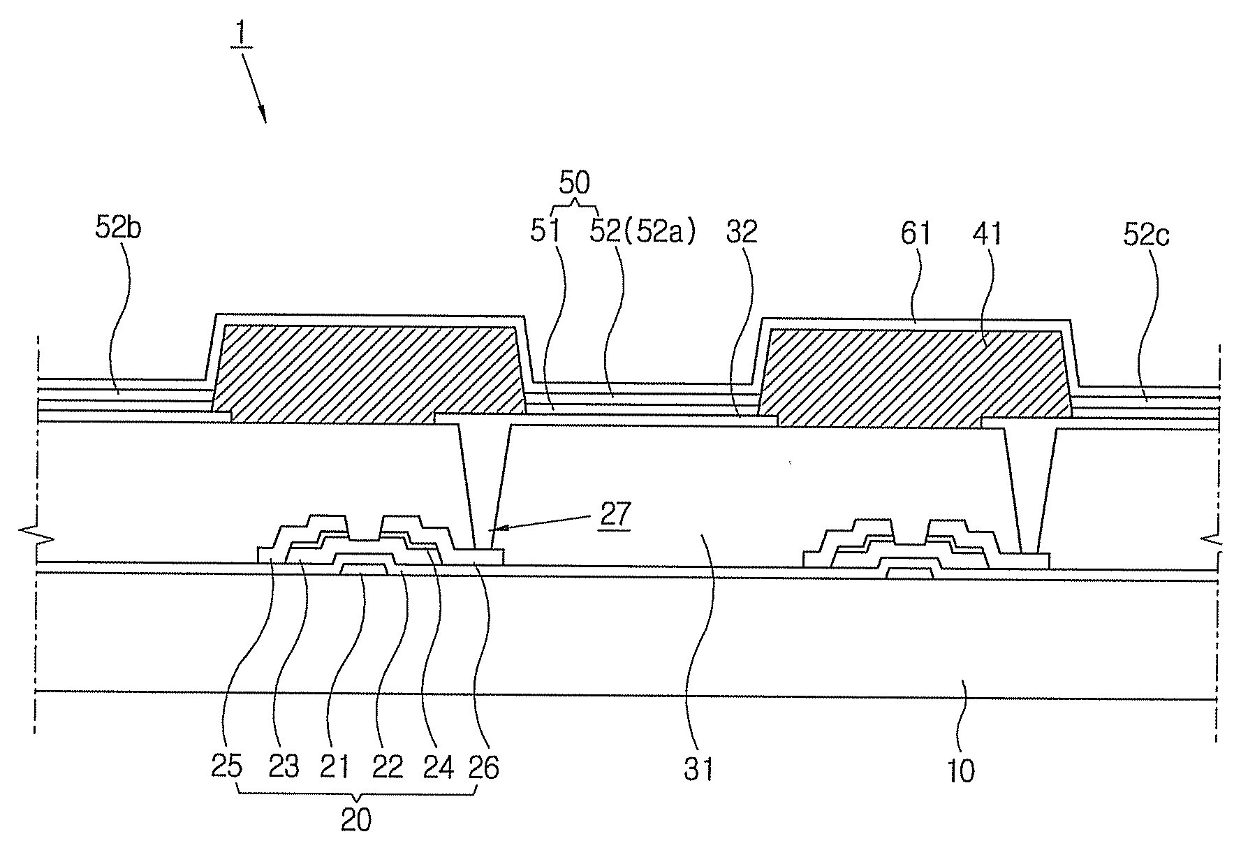
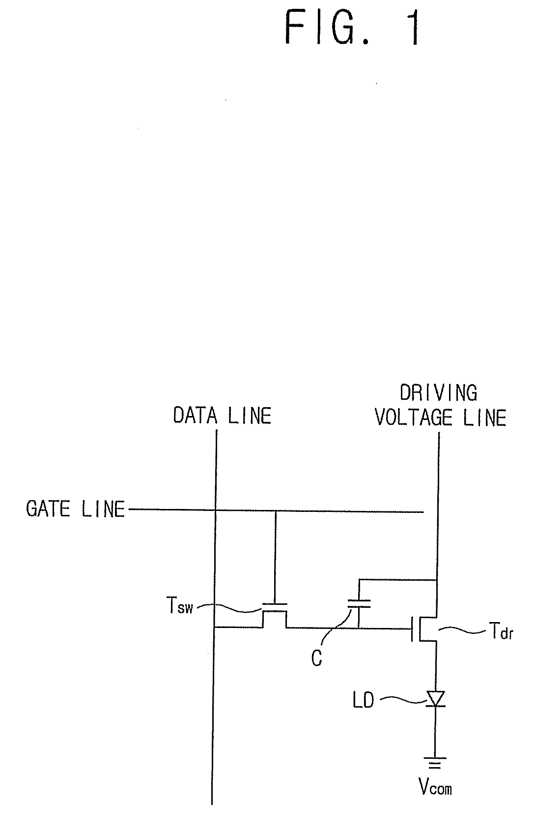
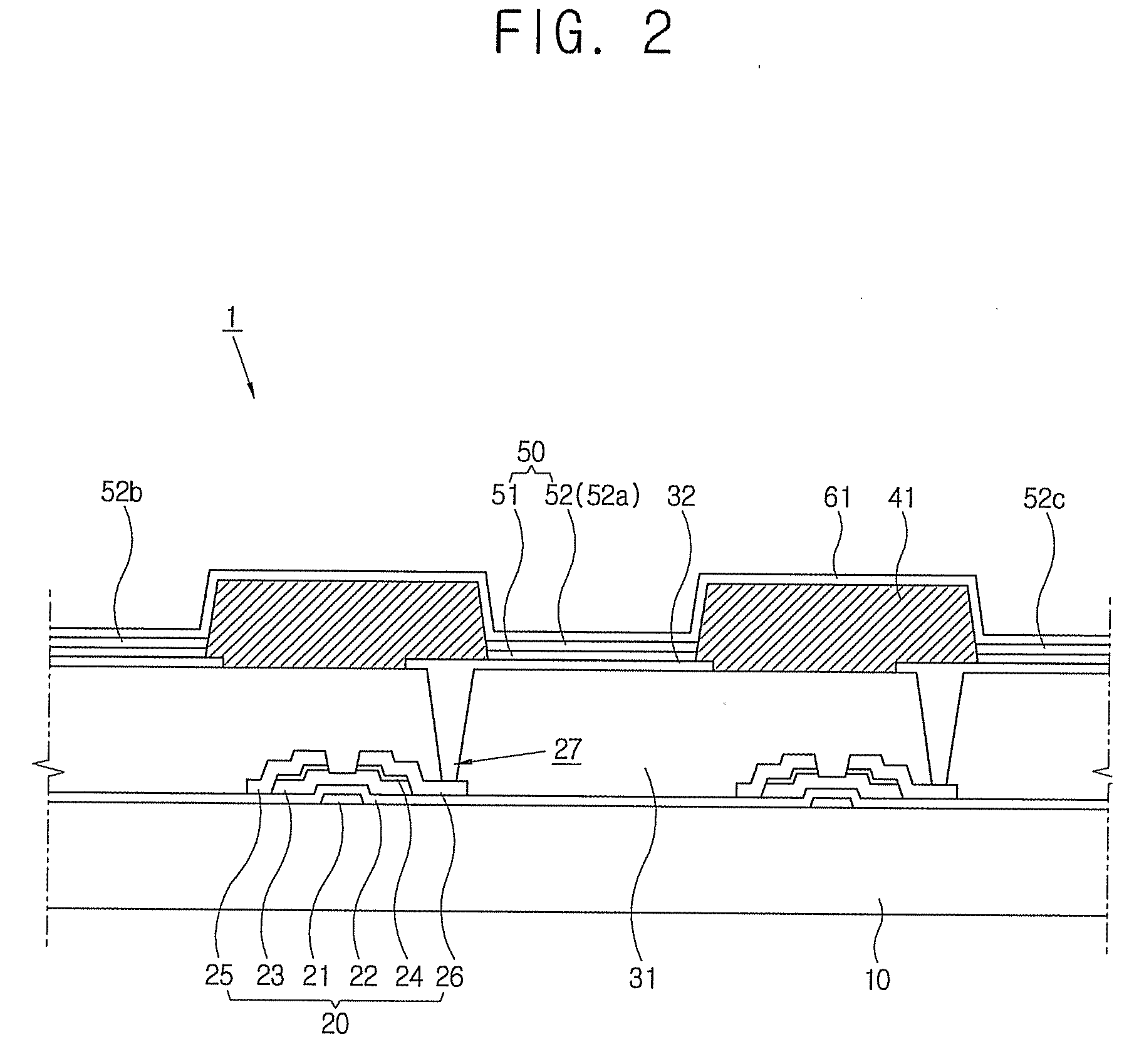
[0041] Hereinafter, embodiments of the present invention will be described with reference to accompanying drawings, wherein like numerals refer to like elements and repetitive descriptions will be avoided as necessary. This invention may, however, be embodied in many different forms and should not be construed as limited to the embodiments set forth herein. Rather, these embodiments are provided so that this disclosure will be thorough and complete, and will fully convey the scope of the invention to those skilled in the art.

[0042] Hereinafter, a term of “on” means that a new layer (i.e., film) may be interposed or not interposed between two layers (i.e., films), and a term of “directly on” means that two layers (i.e. films) are in contact with each other. As used herein, the term “and / or” includes any and all combinations of one or more of the associated listed items.

[0043] It will be understood that, although the terms first, second, third etc. may be used herein to describe var...


PUM


Abstract

A method of manufacturing a display device includes forming a thin film transistor on an insulating substrate, forming an electrode electrically connected to the thin film transistor, forming a wall surrounding the electrode, ejecting ink comprising an organic material and a first solvent on the electrode, and supplying a second solvent to the ink. Thus, an organic layer of uniform quality is formed in the display device formed by the method.

Description

[0001] This application claims priority to Korean Patent Application No. 2005-0114373, filed on Nov. 28, 2005 and all the benefits accruing therefrom under 35 U.S.C. §119, and the contents of which in its entirety are herein incorporated by reference. BACKGROUND OF THE INVENTION [0002] 1. Field of the Invention [0003] The present invention relates to a manufacturing method of a display device and a display device therefrom. More particularly, the present invention relates to a manufacturing method of a display device having an improved organic layer, and a display device therefrom. [0004] 2. Description of the Related Art [0005] Recently, an organic light emitting diode (“OLED”) has become popular since it is driven through a low voltage, is light and small, has a wide viewing angle, and responds with high speed. The OLED is classified into a passive matrix type and an active matrix type according to a driving method. The passive matrix type has a simple production process, but dras...

Claims


Application Information

Patent Timeline
Patent Type & Authority Applications(United States)
IPC IPC(8): H01L51/00
CPCH01L27/3295H01L51/0005H10K71/135H10K59/122H05B33/10
Inventor HA, JAE KOOKJIN, YONG-SUK
Owner SAMSUNG DISPLAY CO LTD
Why Eureka
Try Eureka