Liquid crystal display device

a liquid crystal display and display device technology, applied in the field of liquid crystal display devices, can solve the problems of affecting the quality of the movie, the voltage value is limitative, and the movie is known to be inferior, so as to improve the gradation-viewing angle characteristics, shorten the response time, and improve the effect of the response tim

Active Publication Date: 2007-05-31
SHARP KK
View PDF35 Cites 16 Cited by
  • Summary
  • Abstract
  • Description
  • Claims
  • Application Information

AI Technical Summary

Benefits of technology

[0027] An object of the present invention is to provide a liquid crystal display device capable of further shortening the response time down from one frame period, makin

Problems solved by technology

One possible reason for such low response speed of the liquid crystal display device is that the liquid crystal molecule per se has only a slow response, and cannot make a response within a single frame under low temperatures or low gradation state, and this consequently raises a problem of causing blurring and afterimage in the movie.
The liquid crystal display device uses light from an illumination device placed on the back side for the display, wherein the illumination device is kept active throughout one frame, and is therefore known to be inferior in the movie characteristics as compared with CRT and plasma display device which adopt pulse illumination within one frame.
This is because too high voltage for accelerating the response may result in overshooting which adversely affect the movie display, so that the voltage value is limitative.
For VA-mode liquid crystal panel, a phenomenon has been confirmed in that disturbance in orientation of the liquid crystal molecules becomes serious under high voltage application.
Also the molecules out of alignment may gradually recover the normal alignment with elapse of time un

Method used


Image

  • Liquid crystal display device
  • Liquid crystal display device
  • Liquid crystal display device

Examples


first embodiment

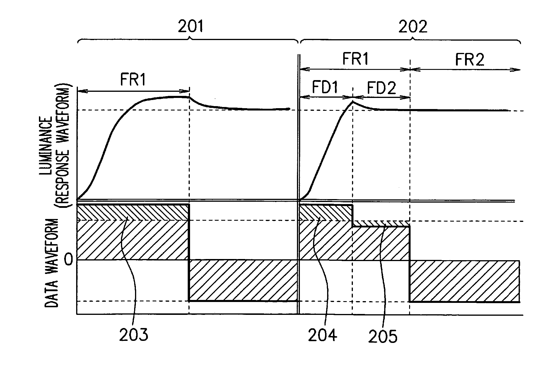
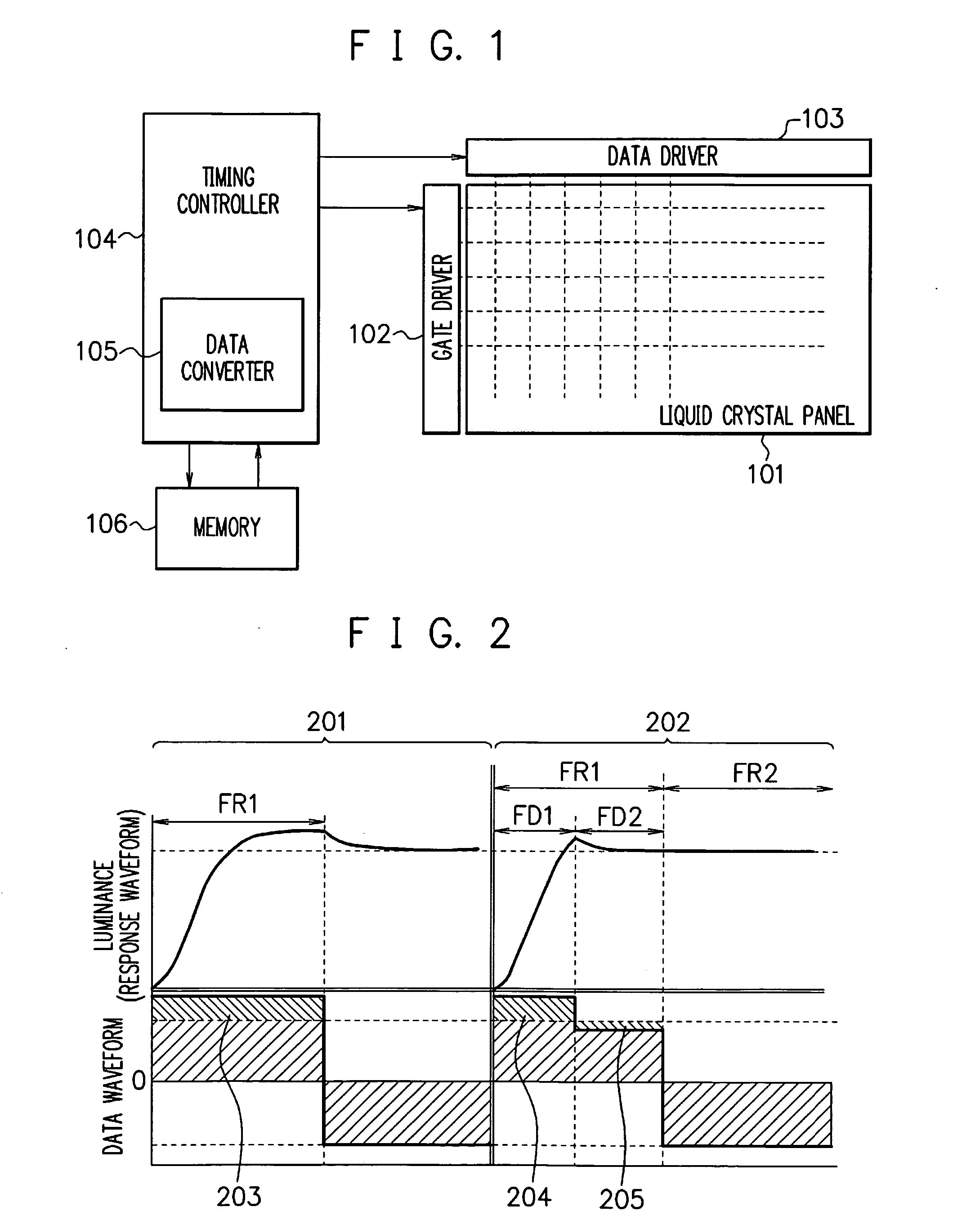
[0038]FIG. 1 is a drawing showing an exemplary configuration of the liquid crystal display device according to the first embodiment of the present invention. A timing controller 104 has a data converter 105, allowing itself to write and read to and from a memory 106. A data converter 105 divides one frame into a plurality of fields, and converts a frame data into a field data. A gate driver 102 supplies, by fields, a gate pulse voltage to gate lines (scanning lines) in a liquid crystal panel 101, under control by a timing controller 104. The gate lines are lines for selecting pixels. A data driver 103 supplies, by fields, a data voltage to data lines (signal lines) in the liquid crystal panel 101, under control by the timing controller 104. The data lines are lines for supplying pixel data. The liquid crystal panel 101 has an array substrate on which a plurality of gate lines and a plurality of data lines are crossed thereon, and an active element (TFT: thin film transistor) is form...

second embodiment

[0046] The first embodiment has aimed at improving the response speed by applying the same data, as the pre-conversion data, to the first field FD1 and the second field FD2, whereas the second embodiment of the present invention will deal with the case where different pre-conversion data will be applied to the first field FD1 and the second field FD2.

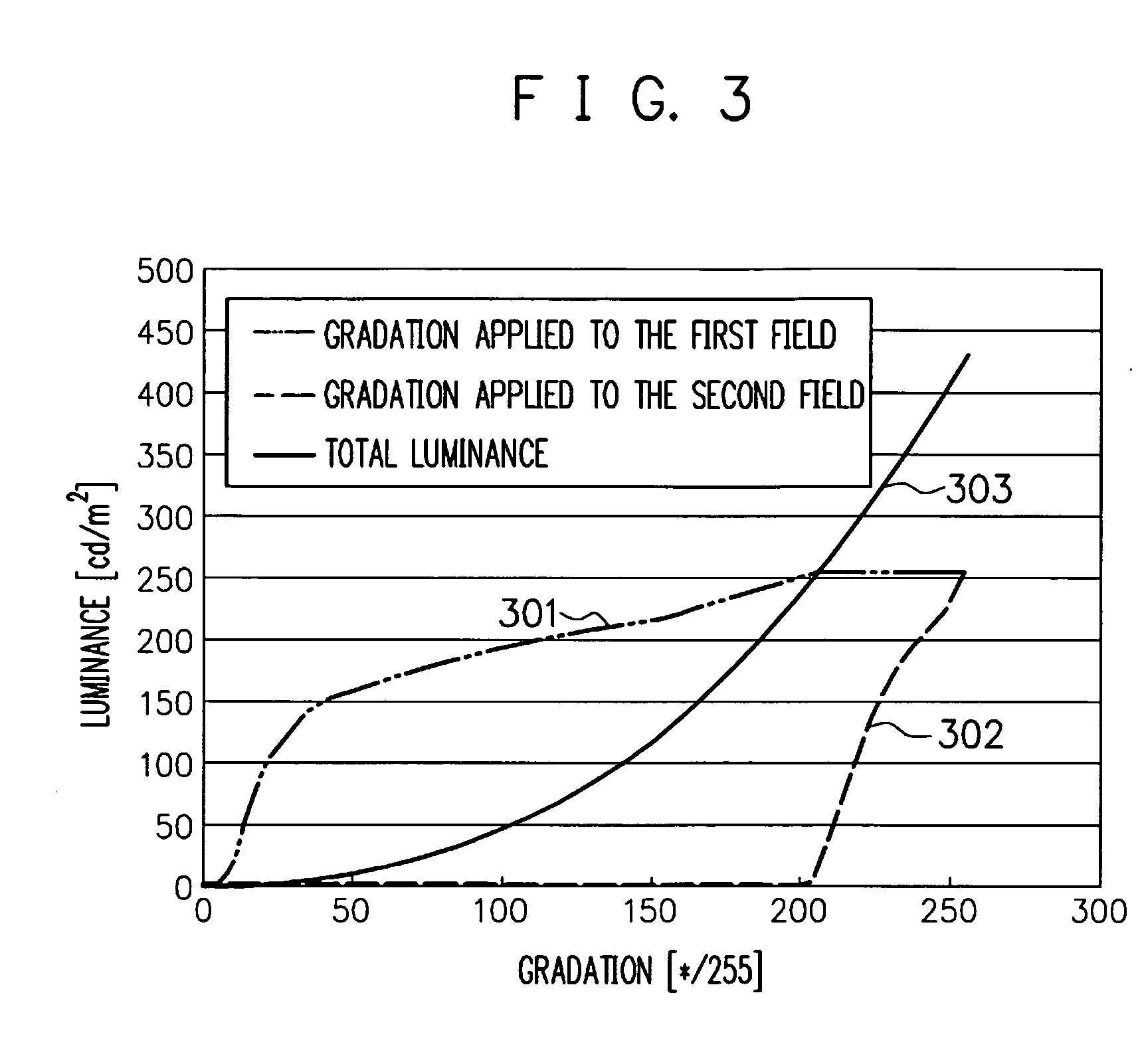
[0047] As the data voltage, V1 is applied to the low-gradation first field FD1, and the black-level voltage (minimum gradation value) Vb are applied to the second field FD2. On the high gradation side, the white-level voltage Vw is applied to the first field FD1, and V3 is applied to the second field. The individual voltage values are selected so that target luminance values can be achieved for the individual frames, by time integral of data voltages V1 and Vb on the low gradation side, and of data voltages Vw and V3 on the high gradation side.

[0048]FIG. 3 is a drawing showing relations between the gradation and the luminance. A chara...

third embodiment

[0063] Division of one frame into two fields can also shorten the write time to the pixels. In 60-Hz operation, the gate pulse time in the normal operation under the XGA resolution is given as 1 / 60 / 768=21.7 μs, whereas division into two fields gives a halved gate pulse time of 10.9 ξs. The gate pulse is applied to the gate lines in a field-by-field manner. It is apparent that one frame divided by n fields can further shorten the gate pulse time.

[0064] A problem possibly raised herein relates to write ability of the TFT. Division of one frame into two fields is aimed at improving the response speed, whereas an insufficient state of write operation is not only unsuccessful in improving the response speed, but also unsuccessful in compensating variation in the driving ability of TFT depending on environment in which the liquid crystal panel is placed, and in ensuring reliability.

[0065] In this case, a multi-scanning operation of the gates is adopted as a method of ensuring a sufficie...


PUM


Abstract

A liquid crystal display aimed at improving response speed, movie characteristics and viewing angle dependence of gradation is provided as having a liquid crystal panel including a plurality of gate lined selecting pixels and a plurality of data lines supplying pixel data, and a data driver dividing one frame into a plurality of fields to thereby convert a frame data into a field data, and supplying the field data to the data line, wherein in the last field out of the plurality of fields, the data line is applied with a first constant voltage, for the frame data ranging from the minimum gradation value to a first gradation value, and in the top field out of the plurality of fields, the data line is applied with a second constant voltage larger than the first constant voltage, for the frame data ranging from a second gradation value to the maximum gradation value.

Description

CROSS-REFERENCE TO RELATED APPLICATIONS [0001] This application is based upon and claims the benefit of priority from the prior Japanese Patent Application No. 2005-151032, filed on May 24, 2005, the entire contents of which are incorporated herein by reference. BACKGROUND OF THE INVENTION [0002] 1. Field of the Invention [0003] The present invention relates to a liquid crystal display device. [0004] 1. Description of the Related Art [0005] Liquid crystal display devices have widely been disseminated as monitor devices of PCs (personal computers) from the viewpoints of their thinness, light-weight and low power consumption, wherein recent expansion of a market of digital television set has raised an increasing demand on TV-use liquid crystal panel capable of realizing high resolution, for which display quality comparable to that of CRT is required. In particular, liquid crystal display device is known to be slow in response speed when compared with CRT, so that it has been understoo...

Claims


Application Information

Patent Timeline
IPC IPC(8): G09G3/36
CPCG09G3/2018G09G3/2081G09G3/3611G09G2310/0205G09G2310/0251G09G2320/0247G09G2320/0252G09G2320/0261G09G2320/028G09G2320/041G09G2320/103G09G2340/16
Inventor TANAKA, RYOKOBAYASHI, TETSUYANAGATANI, SHINPEI
Owner SHARP KK
Why Eureka
Try Eureka