
Light-emitting device and process for manufacturing the same

a technology of light-emitting devices and heat sinks, which is applied in the direction of semiconductor devices, lighting and heating apparatus, lighting apparatus, etc., can solve the problems of degrading the operation quality of the module, increasing the temperature of the module composed of light-emitting devices, and burning out light-emitting devices, so as to increase the heat-sinking efficiency increase the operation stability of the light-emitting device.

Inactive Publication Date: 2007-05-31
NAT CHENG KUNG UNIV
View PDF0 Cites 13 Cited by
  • Summary
  • Abstract
  • Description
  • Claims
  • Application Information

AI Technical Summary

Benefits of technology

The present invention provides a process for manufacturing a light-emitting device by directly forming heat-sinking metal on a light-emitting chip using plating deposition, electroless plating deposition, or evaporation deposition. This eliminates the need for glue to adhere the heat-sinking metal to the chip, improving heat-sinking efficiency and reducing temperature. The process involves using a first adhesive tape to adhere the chip to a temporary substrate, followed by the deposition of a thin metal layer and the formation of a metal heat sink on the chip. The thin metal layer acts as a heat conduction area, increasing the heat-sinking efficiency of the device. The invention also provides a light-emitting device with a thin metal layer directly connected to the chip, improving heat-sinking efficiency and operation stability.

Problems solved by technology

However, when the light-emitting devices are operated at high power, the temperature of the module composed of the light-emitting devices increases, degrading the operation quality of the module and ultimately burning out the light-emitting devices.
However, regarding setting fans in the device, the vibration caused by the operation of the fans results in the lights flickering, and the fans consume additional power.
As a result, the glue acts as a barrier to heat transfer and makes the heat sinks less effective.

Method used


Image

  • Light-emitting device and process for manufacturing the same
  • Light-emitting device and process for manufacturing the same
  • Light-emitting device and process for manufacturing the same

Examples


Embodiment Construction

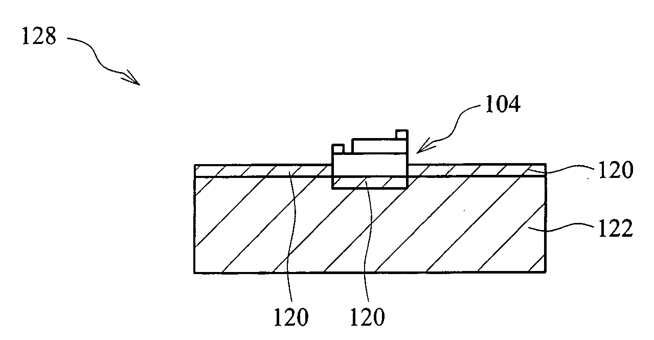
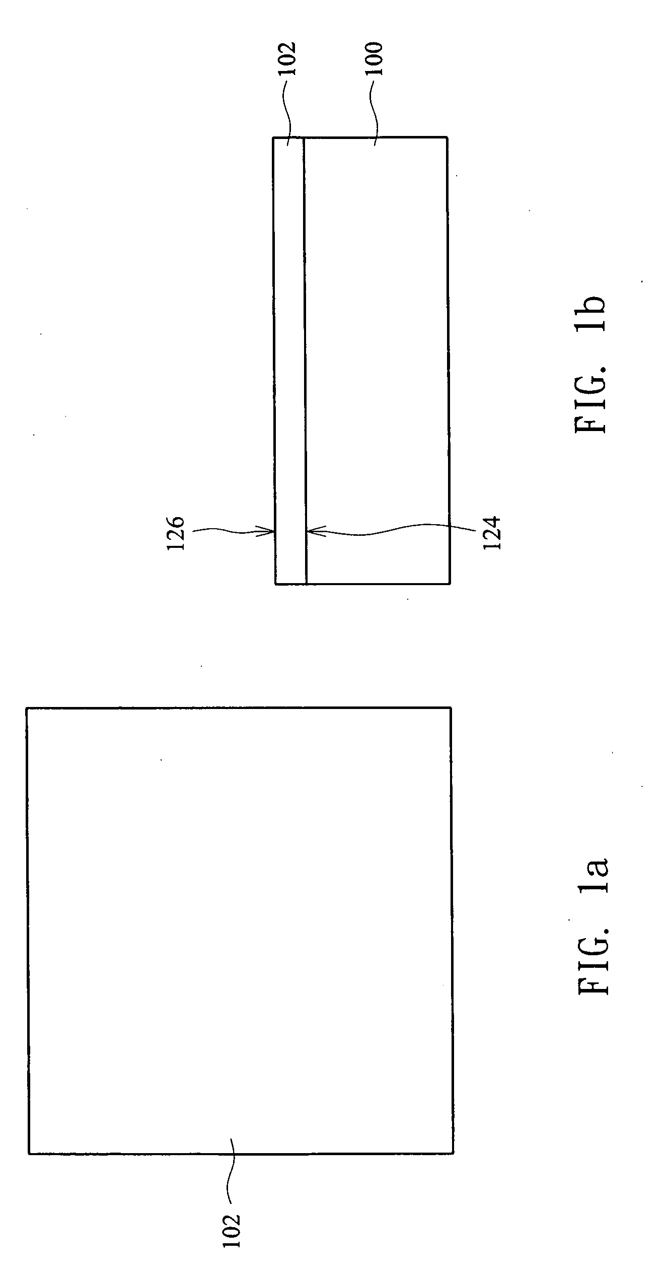
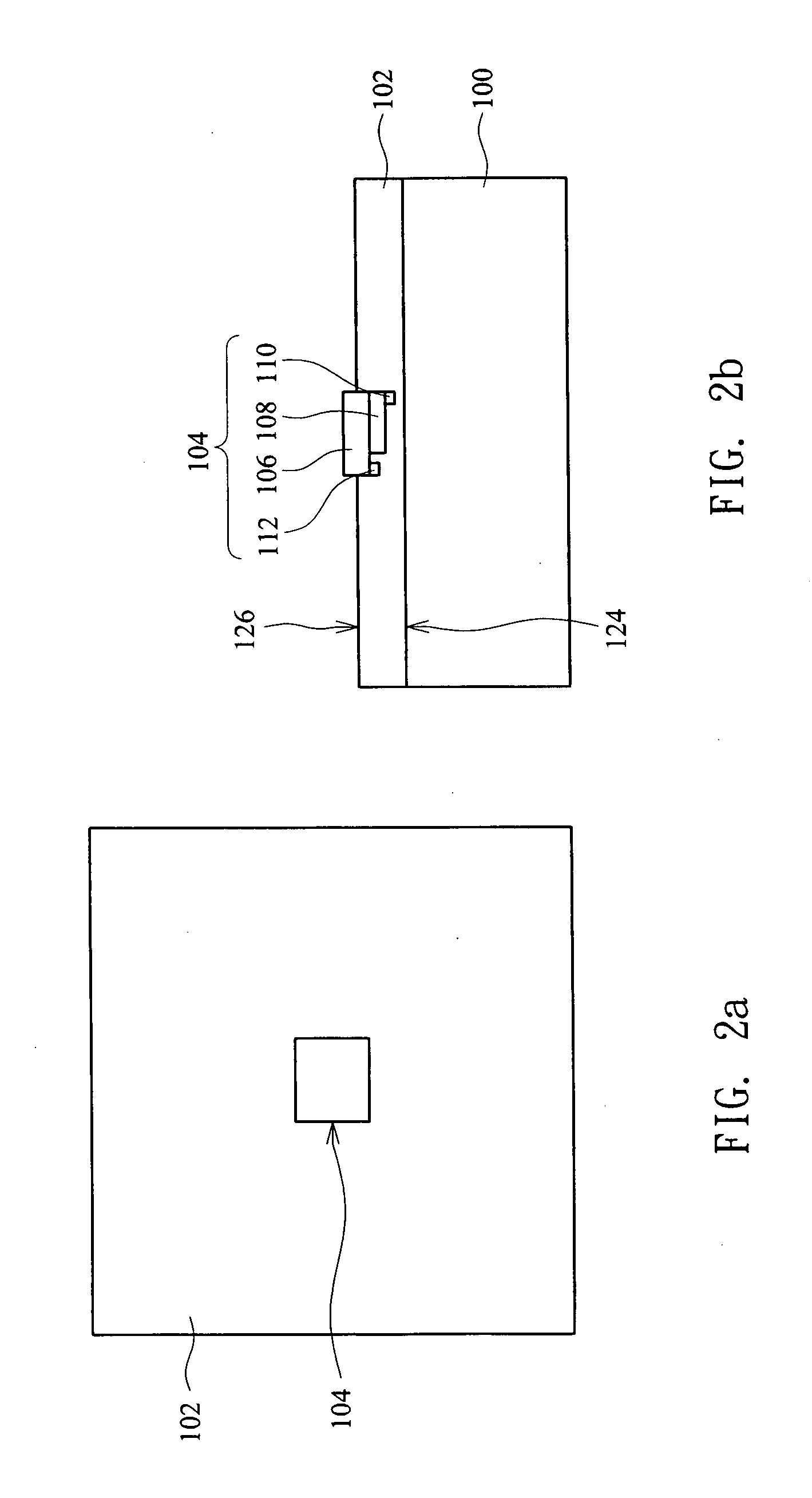
[0016] The present invention discloses a light-emitting device and a process for manufacturing the same, in which a metal heat sink is directly fabricated on the light-emitting chip, so that glue is eliminated, the transmitting area and speed of heat can be greatly enhanced, and the light-emitting device effectively and rapidly dissipates heat. In order to make the illustration of the present invention more explicit, the following description is stated with reference to FIGS. 1a through 7.

[0017]FIGS. 1a through 7 are schematic flow diagrams showing the process for manufacturing a light-emitting device in accordance with a preferred embodiment of the present invention. In the fabrication of the light-emitting device of the present invention, a temporary substrate 100 and a adhesive tape 102 are firstly provided, wherein the adhesive tape 102 includes two surfaces 124 and 126 on opposite sides, and the surface 124 of the adhesive tape 102 is adhered to a surface of the temporary subs...


PUM

PropertyMeasurementUnit
thicknessaaaaaaaaaa
thicknessaaaaaaaaaa
thicknessaaaaaaaaaa

Abstract

A light-emitting device and a process for manufacturing the same are described. The light-emitting device comprises: a thin metal layer including a first surface and a second surface on opposite sides; a metal heat sink directly formed and closely connected to the second surface of the thin metal layer; and a light-emitting chip deposed on a portion of the first surface of the thin metal layer, wherein the thin metal layer directly contacts and is closely connected with the light-emitting chip.

Description

RELATED APPLICATIONS [0001] The present application is based on, and claims priority from, Taiwan Application Serial Number 94142169, filed Nov. 30, 2005, the disclosure of which is hereby incorporated by reference herein in its entirety. FIELD OF THE INVENTION [0002] The present invention relates to a light-emitting device and a process for manufacturing the same, and more particularly, to a method for manufacturing a light-emitting device and a heat sink thereof. BACKGROUND OF THE INVENTION [0003] When small solid state light-emitting devices, such as light-emitting diodes (LEDs) or laser diodes (LDs), are applied in a large or small backlight module or illumination module, a lot of light-emitting devices are needed for the requirements of brightness or illumination of these modules. However, when the light-emitting devices are operated at high power, the temperature of the module composed of the light-emitting devices increases, degrading the operation quality of the module and u...

Claims


Application Information

Patent Timeline
Patent Type & Authority Applications(United States)
IPC IPC(8): F21V29/00
CPCH01L33/641H01L2933/0075
Inventor CHEN, GUAN-QUNLIN, CHUN-LIANGHU, SHU-KAIHUANG, JIN-QUAN
Owner NAT CHENG KUNG UNIV
Learn More