Processing liquid coating apparatus and a processing liquid coating method

Inactive Publication Date: 2007-05-31
EBARA CORP
View PDF9 Cites 4 Cited by
  • Summary
  • Abstract
  • Description
  • Claims
  • Application Information

AI Technical Summary

Benefits of technology

[0014] The present invention has been made in view of the above drawbacks. It is therefore an object of the present invention to provide a processing liquid coating apparatus and a processing liquid coating method which can uniformly coat a surface of a substrate with a small amount of a processing liquid such as a resist liquid or a developer and can perform a replacement of the processing liquid smoothly, and can also prevent a pattern collapse.
[0025] According to the present invention, all portions of the surface of the substrate can be supplied with the processing liquid (i.e., the resist liquid or the developer) at substantially the same time. Therefore, a film (e.g.,a resist film) of the processing liquid can be uniformly formed on the surface of the substrate even if a small amount of the processing liquid is used. Further, because the processing liquid can be supplied over the entire surface of the substrate without utilizing the centrifugal force, the substrate is allowed to rotate at a low rotational speed. Therefore, it is possible to reduce an amount of the processing liquid scattered from the substrate while the substrate is being rotated. Furthermore, by sucking the processing liquid on the substrate and supplying the dry gas to the substrate, the substrate can be dried sufficiently even if the substrate is rotated at a low rotational speed. Therefore, it is possible to prevent the pattern collapse.

Problems solved by technology

However, since the above-mentioned resist coating process utilizes the centrifugal force so as to spread the resist liquid, a large amount of the resist liquid is required to be supplied to the wafer while the excess resist liquid is thrown off the wafer.
Therefore, a much larger amount of the resist liquid is used than is required to form the resist film, thus causing an increased fabrication cost.
Further, in the development process, since the developer is supplied onto the central portion of the resist film (wafer) as with the resist coating process, there is a difference in contact time with the developer between the central portion and the peripheral portion of the resist film, and hence the uniform development cannot be performed.
In addition, although the developer on the wafer is replaced with a new developer by the rotation of the wafer in the above-mentioned development process, the replacement of the developer in the circuit pattern grooves is not performed sufficiently.
Accordingly, the replacement of the developer is not performed smoothly in the circuit pattern grooves, resulting in a non-uniform development and a long development time.
In the rinsing process after the development process, since the replacement of the rinsing liquid is not performed smoothly because of the same reason as described above, the development cannot be stopped as intended, resulting in an excessive development.
Furthermore, in the drying process after the rinsing process, the high-speed rotation of the wafer may cause wall portions constituting the circuit patterns to collapse, which is a so-called pattern collapse.
If the rotational speed is decreased in order to prevent the pattern collapse, the rinsing liquid are likely to remain in the circuit pattern grooves, and hence the wafer cannot be dried sufficiently.

Method used


Image

  • Processing liquid coating apparatus and a processing liquid coating method
  • Processing liquid coating apparatus and a processing liquid coating method
  • Processing liquid coating apparatus and a processing liquid coating method

Examples


first embodiment

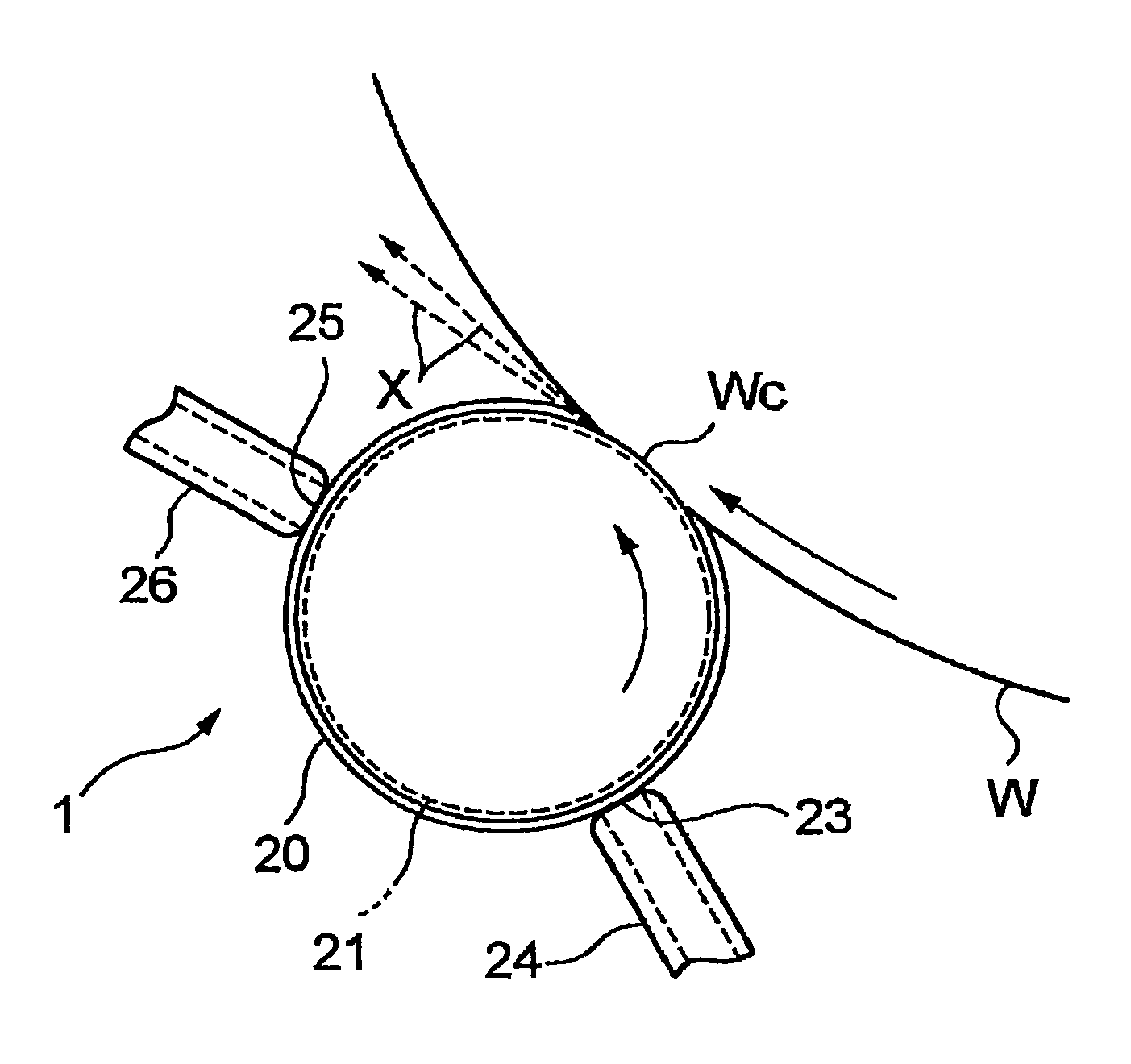
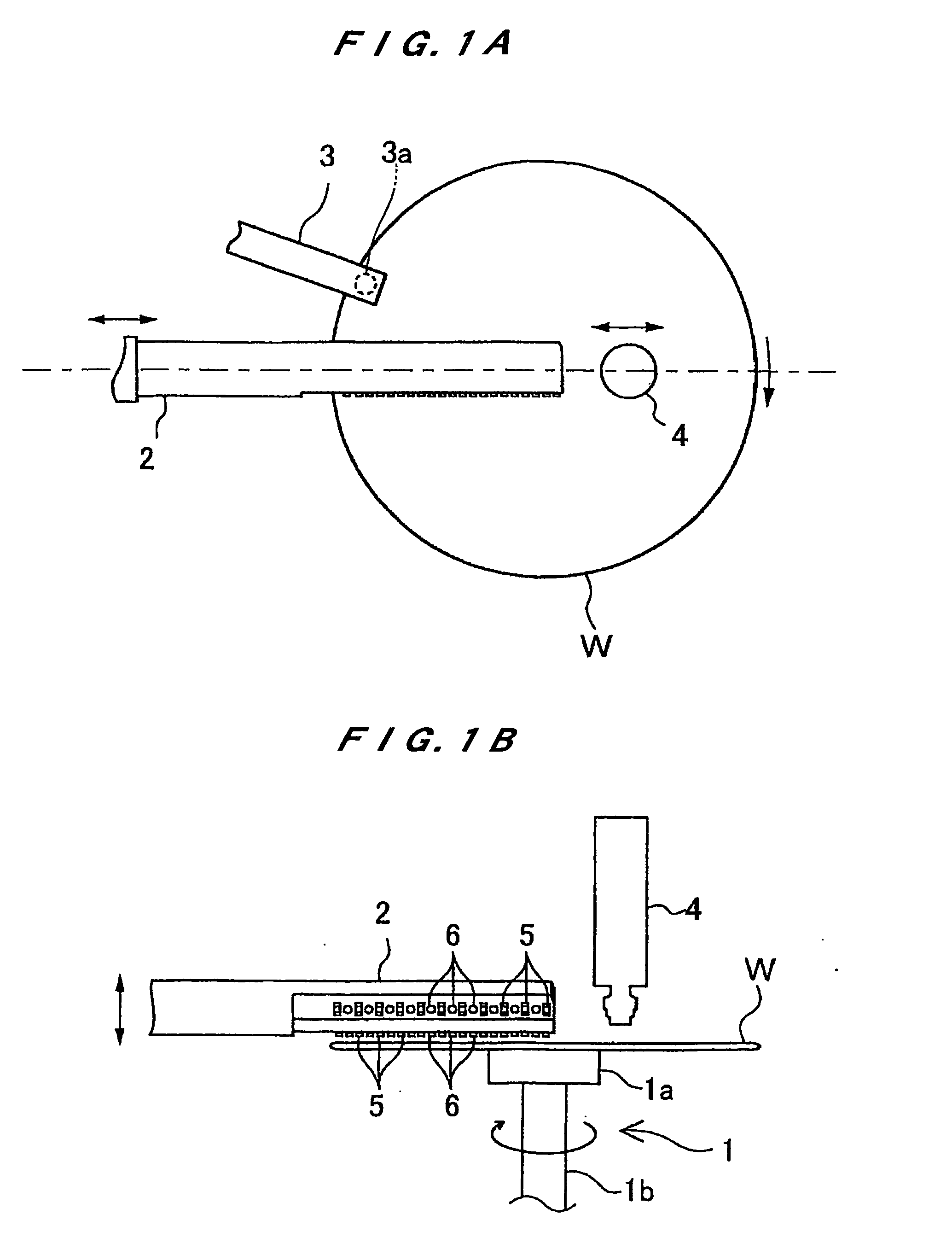
[0039]FIG. 1A is a plan view showing a processing liquid coating apparatus according to the present invention, and FIG. 1B is a side view of the processing liquid coating apparatus shown in FIG. 1A.

[0040] As shown in FIGS. 1A and 1B, the processing liquid coating apparatus comprises a substrate holder 1 for holding and rotating a wafer (i.e., a substrate) W horizontally, a processing liquid supply unit 2 for supplying a predetermined processing liquid onto an upper surface of the wafer W held by the substrate holder 1, a processing liquid suction unit 3 for sucking the processing liquid from a peripheral portion of the wafer W, and a gas supply unit 4 for supplying a predetermined gas to the upper surface of the wafer W.

[0041] The substrate holder 1 comprises a rotating shaft 1a, and a circular chuck table 1b fixed to an upper end of the rotating shaft la. A through hole (not shown) is formed in the rotating shaft 1a and the chuck table 1b so that the wafer W is attracted to an upp...

second embodiment

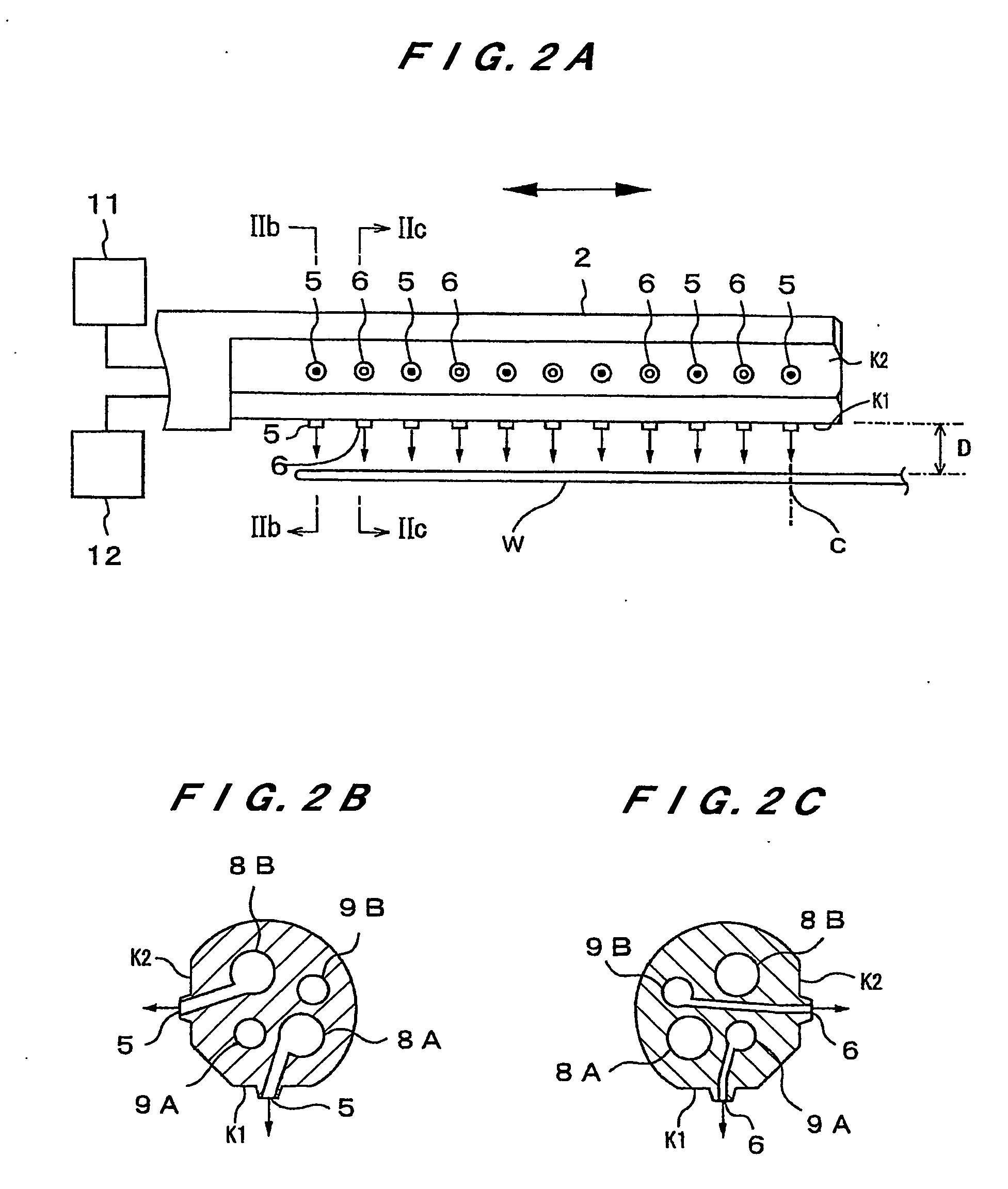
[0069] Next, the present invention will be described with reference to FIGS. 5A through 5C.

[0070]FIG. 5A is an enlarged view showing a processing liquid supply unit incorporated in a processing liquid coating apparatus according to a second embodiment of the present invention, FIG. 5B is a cross-sectional view taken along line Vb-Vb of FIG. 5A, and FIG. 5C is a cross-sectional view taken along line Vc-Vc of FIG. 5A. Components and operations of the processing liquid coating apparatus of this embodiment, which will not be described below, are the same as those of the first embodiment.

[0071] The processing liquid supply unit 2 of the second embodiment has basically the same structure as the first embodiment. However, the second embodiment is different from the first embodiment in that the second communication passages 9A and 9B are connected to the vacuum source 13 through the gas-liquid separator 14 (see FIG. 3). Therefore, the second supply ports 6 communicating with the second com...


PUM


Abstract

The present invention relates to a processing liquid coating apparatus and a processing liquid coating method suitable for use in a lithography process for forming fine circuit patterns on a surface of a substrate such as a semiconductor wafer. The processing liquid coating apparatus according to the present invention includes a substrate holder (1) for holing and rotating a substrate (W), and a processing liquid supply unit (2) disposed apart from the substrate (w) held by the substrate holder (1). The processing liquid supply unit (2) has a plurality of supply ports (5, 6) for supplying a processing liquid to a plurality of portions including a central portion (C) of a surface of the substrate (W). A resist liquid or a developer is used as the processing liquid.

Description

TECHNICAL FIELD [0001] The present invention relates to a processing liquid coating apparatus and a processing liquid coating method, and more particularly to a processing liquid coating apparatus and a processing liquid coating method suitable for use in a lithography process for forming fine circuit patterns in a surface of a substrate such as a semiconductor wafer. BACKGROUND ART [0002] In a semiconductor fabrication apparatus, a lithography process is conducted for forming fine circuit patterns in a surface of a substrate such as a semiconductor wafer. This lithography process involves a combination of a resist coating process for forming a resist film on a surface of a wafer, a pattern exposure process for transferring circuit patterns to the resist film, and a development process for forming circuit pattern grooves in the resist film along the transferred circuit patterns. Hereinafter, there will be described the resist coating process, the pattern exposure process, and the de...

Claims


Application Information

Patent Timeline
IPC IPC(8): G21H5/00H01F41/00G21H1/00B01J19/08B05C11/00B05C11/08B05D1/40G03F7/16G03F7/30H01L21/00H01L21/027H01L21/687
CPCG03F7/162G03F7/3021H01L21/6715H01L21/68707H01L21/68728B05D1/40
Inventor SHIRAKASHI, MITSUHIKOHIROSE, MASAYOSHI
Owner EBARA CORP
Why Eureka
Try Eureka